
Simple adjustment of high input impedance double wave linear detection circuit RC4558DN

The described circuit operates as a high input impedance double wave linear detector, utilizing an operational amplifier (op-amp) for signal processing. The circuit's configuration allows it to rectify both halves of an AC signal while maintaining minimal distortion due to its high input impedance. The operational amplifier A1 is primarily responsible for processing the input signal, with its output fed back through a negative feedback loop, which stabilizes the gain and ensures linearity across the signal range.
The diodes D1 and D2 serve as rectifying elements, enabling the detection of both positive and negative cycles of the input AC signal. When the input signal is in its positive half-cycle, A1 outputs a positive voltage, which forward-biases D1, allowing current to flow and providing a corresponding positive voltage to the non-inverting input of A2. This configuration results in a positive output from A2, reinforcing the signal through the feedback network formed by R1, R2, and VR1, effectively setting the gain to -1.
Conversely, during the negative half-cycle, A1's output becomes negative, causing D1 to reverse bias. In this state, the input to A2 drops to zero, and the operational amplifier A1 transitions to function as a voltage follower due to the feedback through D2. This arrangement ensures that the input and output voltages of A2 remain equal while maintaining a gain of 1.
The presence of the variable resistor VR1 allows for fine-tuning of the circuit's gain characteristics, accommodating variations in the input signal or component tolerances without the need for precision resistors. This flexibility is crucial in applications where signal integrity and fidelity are paramount, such as in audio processing, instrumentation, or communication systems. Overall, this circuit design exemplifies a robust solution for high input impedance detection with adjustable gain characteristics, suitable for a variety of electronic applications. As shown for the simple adjustment of the high input impedance double wave linear detector circuit. The operational amplifier circuit by the negative feedback loop to compensat e for non-linear diode installed mobile feedback level Vf. Circuit without the use of precision resistors, which is characterized by the gain difference can easily be compensated for by the positive and negative input adjustment VR1 approach. Since the signal from the inverting terminal A1 input, the input impedance is high, it does not appear nonlinear distortion.
Enter positive half cycle of the AC signal, the output of A1 is positive, D1 is forward biased and is turned on, it is also a positive input A2, A2 output is also positive, with R2, VR1, R1 to be A1 beta negative 1 feedback, in general, into a gain of inverting amplifier 1. In this case, when the gain adjustment VRl unchanged. When the input signal is negative half-cycle, A1 output is also negative, D1 is reverse biased, A2 input to 0, the inverting amplifier A2 becomes.
In this case A1 through D2 negative feedback, in fact, it becomes a voltage follower, inverting input and A2 input AC voltage is the same, while working as a gain for the inverting amplifier A2 1. In this case, the gain can be varied to adjust the VR1 A2, adjusting VR1 so that the overall gain is unity.
Related Circuits
Most CD-ROMs available have an audio output that allows for the connection of headphones or an amplifier. This circuit enables the use of the CD-ROM as a standalone audio CD player without requiring a computer. The circuit essentially functions...
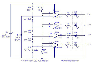
This circuit is a practical device that, when installed in a vehicle, displays the voltage of the car battery using an LED dot display. The meter circuit utilizes four comparators formed from a quad op-amp, specifically the LM324. The...
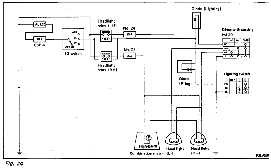
Understanding the headlight wiring in a car involves examining the purpose of two diodes in the circuit diagram. The circuit allows for two independent methods of activating the light relays: through the light switch or by flashing the high...
The name of our game, LED Zeppelin, is a play on words. It comes not from the pop group of the same name but from Graf Von Zeppelin, a German who invented the first rigid air ship in 1900....
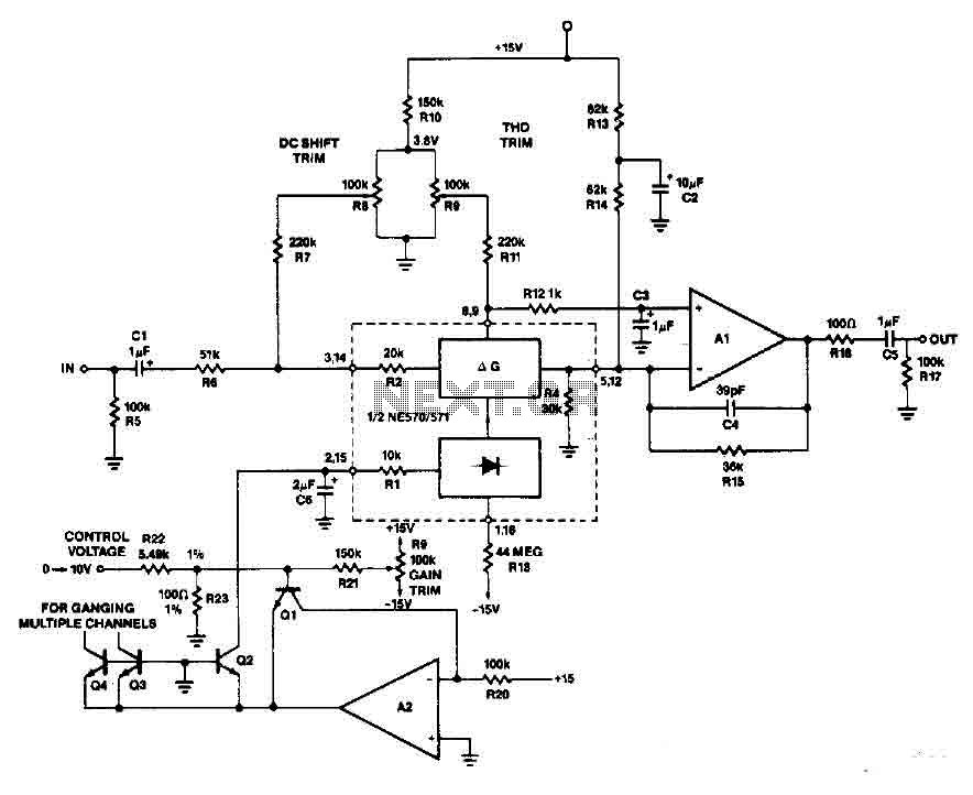
An operational amplifier along with transistors Q1 and Q2 forms an exponential converter to produce an exponential gain control current, which is fed into the rectifier. A reference current of 150 pA, with a voltage of 15 V and...
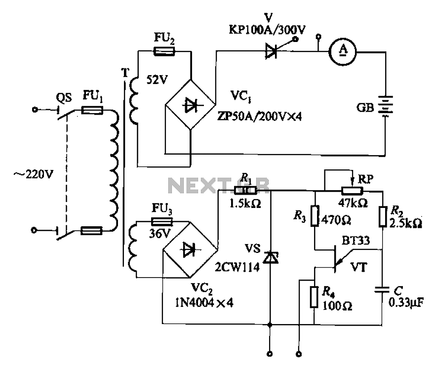
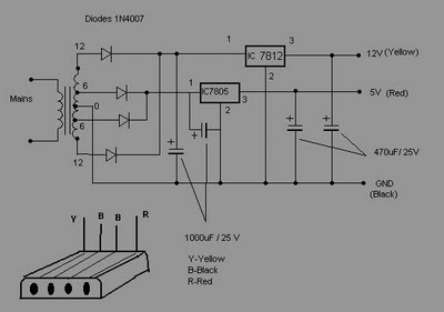
The adjustment potentiometer RP can modify the magnitude of the DC output voltage. The adjustment potentiometer, designated as RP, is an essential component in various electronic circuits, particularly in power supply systems and signal conditioning applications. It serves as a...