
12 V High current regulator

The voltage regulator circuit described operates efficiently to provide a stable output voltage of approximately 11.3V with a maximum current output of 3A. The transformer T1 plays a crucial role by stepping down the high mains voltage to a lower voltage level of 12V RMS, which is essential for safe operation within the circuit. The rectifier bridge D1, typically composed of four diodes arranged in a bridge configuration, converts the AC voltage from the transformer into pulsating DC voltage. This pulsating DC is then smoothed out by capacitor C1, which acts as a filter to reduce voltage ripple, ensuring a more stable DC output.
The use of a series pass transistor, specifically the 2N3055, allows the circuit to handle higher current loads. The biasing of Q1 through resistor R1 ensures that the transistor operates in the active region, allowing it to regulate the output voltage effectively. The zener diode D1 is critical in this configuration as it sets the reference voltage at 12V. When the voltage across the zener diode reaches this threshold, it enters the breakdown region, allowing current to flow and stabilizing the output voltage.
In practical applications, it is important to consider thermal management for the 2N3055 transistor, as it can generate significant heat when operating near its maximum current rating. A suitable heatsink should be used to dissipate heat effectively, ensuring reliable operation over extended periods. Additionally, the circuit may require further components for protection against overcurrent and voltage spikes, such as fuses or transient voltage suppressors, to enhance reliability and safety. Overall, this voltage regulator circuit is a robust solution for applications requiring a stable DC output with relatively high current demands.This voltage regulator circuit can deliver up to 3A at 12V output voltage. The circuit can be employed on occasions when a current of more that 3A is demanded for regulator. IC regulators of such high current rating are pretty hard to find. The transformer T1 steps down mains voltage, to 12rms & the rectifier bridge D1 rectifies it to produce a DC voltage. The C1 filters the rectifier output and produces a DC level. The series pass transistor Q1 (2N 3055) is biased by resistor R1 (680 ©). Since zener diode D1 is under breakdown region the voltage across it will be 12V. So the total output voltage will be steady 11. 3 V(theoretically). That is the zener voltage minus base emitter voltage of Q1. Here transistor Q1 will conduct the excess current required. 🔗 External reference
Related Circuits
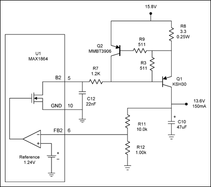
A detailed discussion on implementing current limiting or foldback current limiting for the linear regulator controllers of the MAX1864. This can also be applied to other discrete regulator designs, including the MAX1865, MAX1964, MAX1965, MAX8513, and MAX8514. To incorporate current...
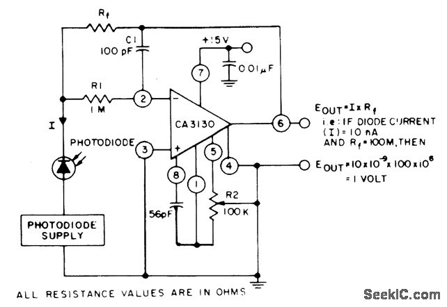
The circuit employs three CA3130 BiMOS operational amplifiers in an application that is sensitive to sub-picoampere input currents. It generates a ground-referenced output voltage that is proportional to the input current flowing through the photodiode. The described circuit utilizes three...
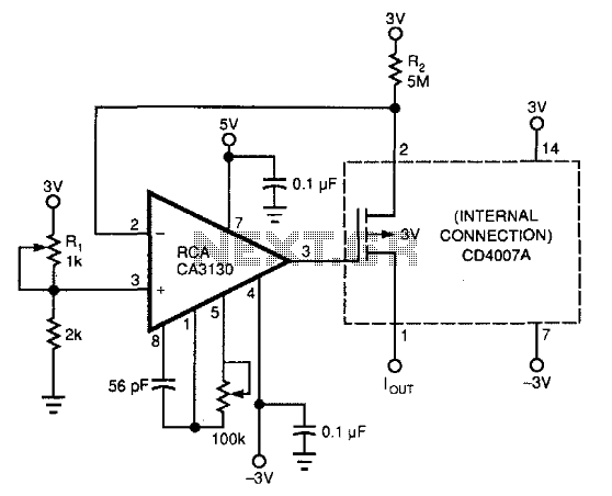
This circuit utilizes commonly available components to create a 0-to-200-nA current source. It incorporates a PMOS transistor from the input stage of a DC4007A, which is more accessible than a standalone PMOS transistor. The CA3130 operational amplifier functions as...

This is an application circuit for calibration known as a high voltage AC calibrator circuit. An essential aspect of sine wave oscillator design is the stable control of amplitude. This circuit not only stabilizes the amplitude through servo control...
This is a Variable Voltage Regulator Circuit built using the LM317T integrated circuit (IC). The LM317T is an adjustable three-terminal positive voltage regulator capable of supplying more than 1.5 amps over an output range of 1.25 to 37 volts....
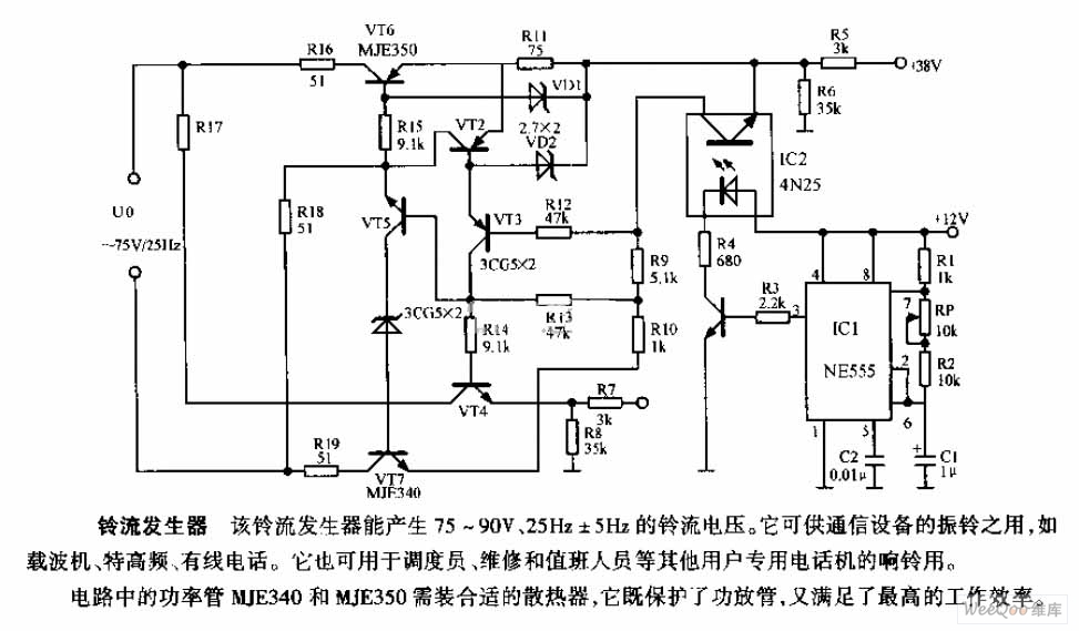
The ring current generator can produce a ringing current voltage of 75-90V and 25Hz ± 5Hz. It is suitable for use in vibrating rings in communication devices, such as carriers, ultrahigh frequency systems, and wire telephones. Additionally, it can...