
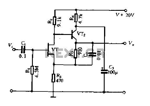
12dB-oct by the OP amplifiers low-pass filter

The 12dB/oct Butterworth filter is characterized by its smooth frequency response and minimal ripple in the passband. The design aims to achieve a Q factor of 0.707, which is critical for maintaining the desired flatness of the filter's response. The feedback capacitance plays a pivotal role in establishing the filter's characteristics and must be chosen carefully to ensure that the desired Q value is attained. The relationship between the components in the circuit is crucial; for instance, the feedback capacitance (Cl) and the resistance (R) must be properly calibrated to maintain the integrity of the signal while minimizing distortion.
The cut-off frequency of the filter can be adjusted, providing some design flexibility. However, care must be taken to avoid excessively high resistance values, as this can lead to operational amplifier input bias offsets that may affect performance, particularly in audio applications. The feedback loop is essential for compensating for these biases, and the choice of an FET input operational amplifier can significantly reduce the input bias current, thus enhancing the overall performance of the filter.
Capacitor C3 serves an important function in the circuit by suppressing voltage spikes that could adversely affect the filter's operation. The selection of its capacitance is also critical; a range of 22 µF is suggested, with the upper limit determined by the specific application requirements. Overall, the design of this Butterworth filter circuit requires careful consideration of component values and relationships to achieve the desired performance characteristics.12dB/oct Butterworth second port (most flat characteristic) of the filter circuit value is pregnant shall be 0.707 to get the characteristic flat, and for cl, the feedback capa citance roar should be taken to ensure high-capacity reaches a predetermined opening value oQ value from the mouth/mouth iTC,/2 formula. In order to make the port 0. 707, a. And c soil must be established cl 4QI. I 2aI the mouth broom relationship. When calculating the effective parameters, according to CI 2 of mouth/2 Xiao, workers Island, Port I 1/2 port x2 help, a worker Xiao calculated sampling D, and oyster I5il not vend, this week can mound up checking Q value.
Although the cut-off frequency is selected with a certain degree of freedom, but the resistance Ro is too large, it will generate the OP amplifier input bias offset by the impact of speech, accrual calculation, chu o, analyze whether there is a problem here feedback loop plus R, to offset the input bias current, if the choice of FET input ol) amplifier, the input bias current is very small, only a few hundred microamps spread can to remove chu 3. c3 role is to suppress spikes, the choice of its capacity range of 22 ~ sipFo
Related Circuits

This circuit utilizes a switched capacitor filter integrated circuit (IC) from National Semiconductor to filter signals with frequencies exceeding 3 kHz, which are not required for voice audio. The circuit design incorporates a switched capacitor filter IC, which is a...

An automatic cooler fan for amplifiers is a circuit designed to conserve power in amplifier circuits. This circuit activates the fan. The automatic cooler fan circuit for amplifiers operates by utilizing temperature sensors to monitor the heat generated by the...
The Field Effect Transistor (FET) exhibits a high input impedance, allowing the construction of high input impedance amplifiers. However, as a FET amplifying device, the distributed capacitance and the Miller effect significantly increase input capacitance at high frequencies. Furthermore,...
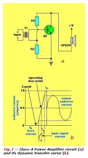
An audio power amplifier can enhance weak signals from devices like tuners, CD players, or tape decks to fill a room with sound. This article emphasizes the operating principles and circuitry of low-frequency power amplifiers utilizing bipolar junction transistors...
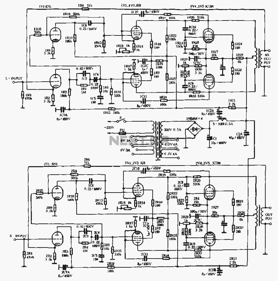
A standard linear amplifier is designed according to a conventional circuit configuration, with the power of the beam tube indicated in Figure 1-8. The output stage employs power tubes such as EL34, KT88, and KT100, which are types of...
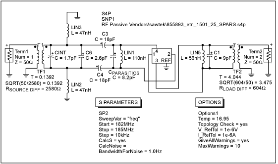
A 183.6 MHz SAW filter is utilized in a CDMA application. The S-parameter of the SAW filter is employed to simulate the interaction with the mixer. An example is provided using the SAWTEK 855893 SAW filter. This application note...