
12kW PFC Boost Converter
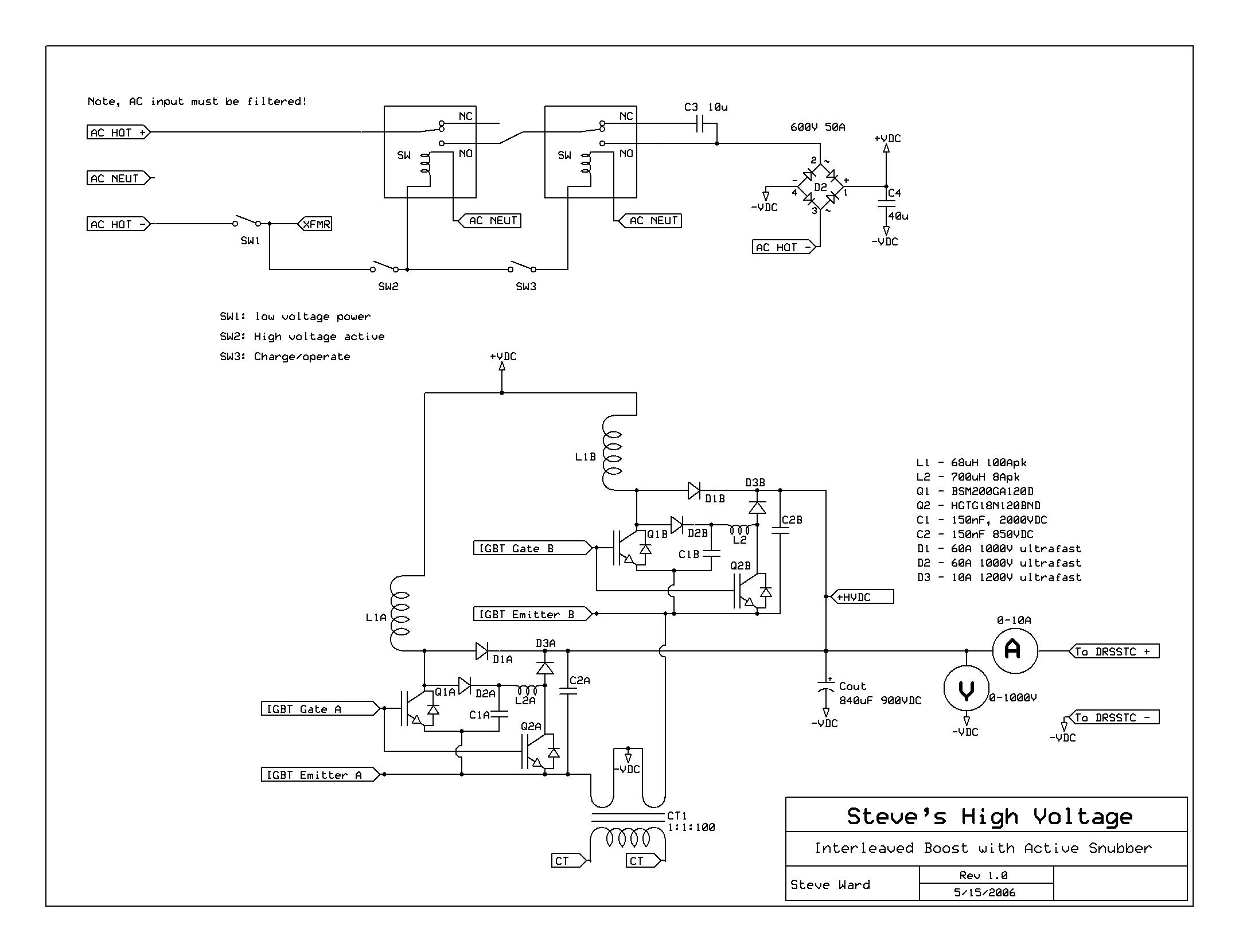
The circuit design incorporates a dual interleaved boost converter topology, effectively distributing the load between two converters to enhance efficiency and reduce thermal stress on individual components. Each converter operates at a maximum of 6kW, with an active snubber circuit that recycles energy, thus minimizing losses associated with IGBT switching. The active snubber not only lowers the thermal burden on the IGBTs but also contributes to overall system efficiency by utilizing the energy stored in the snubber capacitor.
The IGBT switching strategy is critical, focusing on minimizing turn-off losses by ensuring that the voltage across the IGBT is clamped to zero during the turn-off transition. This is achieved through the strategic placement of a capacitor and a series diode, which prevents reverse current flow. The use of current transformers for monitoring allows for real-time feedback to the control system, ensuring that the system can react swiftly to overcurrent conditions, thereby protecting the IGBTs from potential damage.
The implementation of a full-wave rectifier at the output of the CT allows for accurate monitoring of the current flow, ensuring that the control logic can respond appropriately to any anomalies. The design emphasizes a balance between performance and reliability, with careful consideration given to thermal management and component ratings. This project represents a significant advancement in high-power boost converter technology, demonstrating the feasibility of operating at high efficiency while managing complex dynamic conditions.The project is a continuation of the 5kW Boost converter project. After a few failed attempts, I realized that I was really after more power, perhaps 10kW or so. I changed the title from 12kW to 8kW. While the converter is designed for 12kW, its very unlikely that I will ever run at that power level. So I expect the maximum output power to be 800V DC at 10ADC, so 8kW. Discontinuous current, power factor correcting boost converter. 2 converters are interleaved, each operating at 6kW maximum input power. There is an "active" snubber circuit that recycles snubber energy, this greatly reduces IGBT switching loss. Because the converter operates in a discontinuous mode, this implies 2 particular conditions. Firstly, the peak current will be about twice that of a continuous mode converter. Secondly, because the IGBTs don`t turn on with any current, we only care about the turn OFF losses, which will be quite high if not taken care of.
The Turn OFF loss is caused by the instantaneous overlap of the IGBT voltage and current (in this case 850VDC and 100A). This overlap is very short, but can cause quite a bit of loss, which equates to hot IGBTs. The trick is to then place a capacitor across the IGBT so that the instantaneous voltage at shut off, is 0V, that is, until the capacitor gets charged.
There is a diode in series with the capacitor, so that it could never discharge back through the IGBT when it turns ON. The problem then becomes: what to do with the energy in this capacitor A typical snubber places a resistor in parallel with this capacitor to drain off the charge.
In this case, we are basically shifting the IGBT losses to power dissipated in this resistor. The nice thing is that we can locate said resistor remotely, but still, we have to get rid of that heat. My approach is to, instead, make use of this energy stored in the snubber capacitor. Basically, this capacitor becomes the "power supply" for another small boost converter. The capacitors energy is dumped into a small inductor (through another IGBT). When the IGBT opens up, the energy in the inductor is forwarded to the main output capacitor of the converter.
My pspice simulations showed a dramatic drop in power loss. With no snubber circuit employed, IGBT losses totaled around 850W. With the active snubber, the total IGBT loss dropped to an amazing 200W, while delivering 12kW! Obviously, 200W is a lot easier to deal with than 850W, though will still require a considerable amount of cooling (consider a typical computer CPU dissipates 50-70W). In order to keep the IGBTs safe, and to avoid saturation of the main inductors, I needed a way to monitor the current through them.
Richie Burnett set me straight on how to use CTs to monitor this current (which has a DC component!). If I was using a single converter, the trick would be to use a diode in series with the CT output, so that the core would "reset" on every negative current pulse.
But, since I am using 2 converters, I can feed them both through the CT, but in *opposing* direction. This keeps the v*s balanced. I then need to use a full-wave rectifier on the output of the CT. If the CT voltage exceeds the preset reference voltage, the controller ends the pulse right there, shutting off the IGBT.
The controller (nicely) makes sure that the pulse width sent out from A is the same length that B will put out, and vice-versa. So if the current trips on pulse A, then pulse B will be that same truncated length. Finally I have reached the most exciting part of the project, actually seeing if the darn thing works!
A few weeks back I tested the converter with a bucket of slightly salty water as a dummy load. I ran it up to 4900W output (that`s 780V at 6. 3A). I only ran for about 25 seconds since I was producing what appeared to be a good amount of hydrogen through electrolysis. The most recent test was on 5/28/06 where I actually powered up my DRSSTC-2 with the power supp 🔗 External reference
Related Circuits
Boost 3.5V regulator circuit. This chip can boost or create a stable voltage supply from approximately 3V DC to a DC voltage of 3.5V. The boost regulator circuit is designed to increase a lower DC voltage, specifically from around 3V...
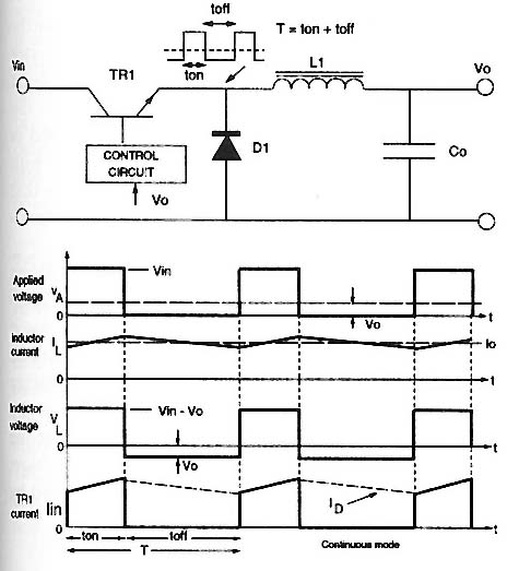
The buck converter circuit serves as the foundation for various similar circuits, known as forward converters. The configuration of the buck converter, along with its input and output voltages, is illustrated in Figure 1. This circuit is typically connected...
This non-isolated, unregulated converter with minimal components serves as a bridge between low-power zener regulation and the higher power applications of a 60-Hz input transformer. It is designed for scenarios where a non-isolated power supply can be utilized safely....
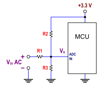
The ATtiny24 microcontroller's ADC is utilized to record an AC signal, which operates within a voltage range of 0 to 3.3V. A precision rectifier is employed to eliminate the negative portion of the signal. The circuit incorporates an LMC6484...
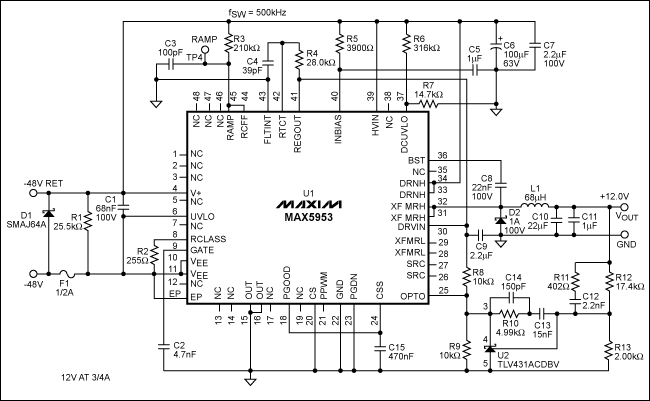
The MAX5953A offers a straightforward, cost-effective, and comprehensive non-isolated power integrated circuit (IC) solution for Powered Devices (PD) in Power-over-Ethernet (PoE) systems. The MAX5953A is designed to facilitate the implementation of Power-over-Ethernet applications by providing an efficient means of...
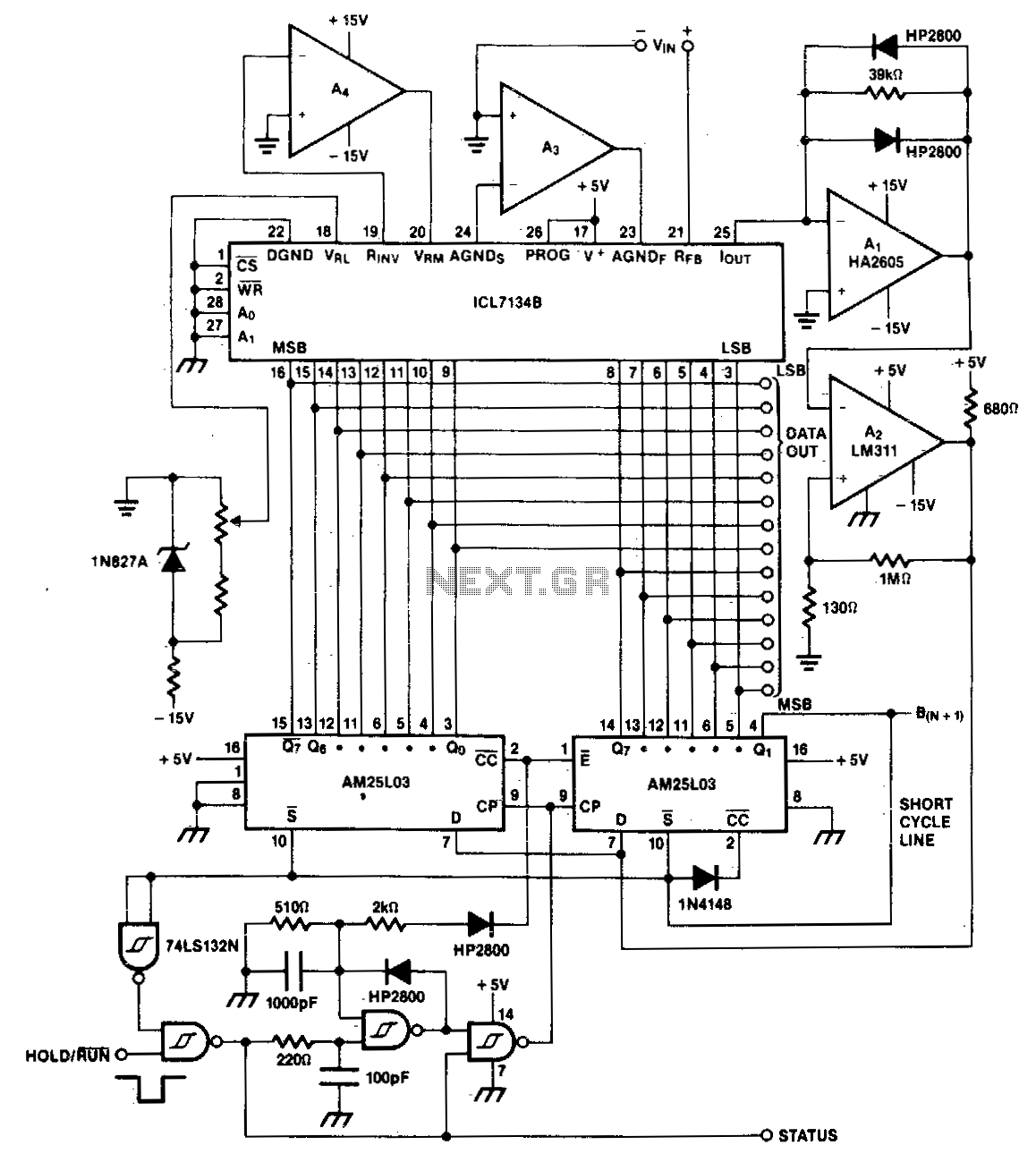
A bipolar input, high-speed A/D converter utilizes two AM25L03 devices to create a 14-bit successive approximation register. The comparator consists of a two-stage circuit featuring an HA2605 front-end amplifier, which is employed to minimize settling time issues at the...