
Boost 3.5V regulator circuit

The boost regulator circuit is designed to increase a lower DC voltage, specifically from around 3V to a stable output of 3.5V. This circuit typically employs a switching regulator topology, which is efficient for converting voltage levels while minimizing power loss.
The primary component of this circuit is a boost converter IC, which integrates various functionalities such as a switching transistor, control logic, and feedback mechanisms. The input voltage is fed into the circuit, where it is stored in an inductor during the 'on' state of the switching cycle. When the switch turns 'off', the inductor releases its stored energy, which is then transferred to the output capacitor, raising the voltage to the desired level.
Key components of the circuit include:
1. **Inductor**: This stores energy when the switch is closed and releases it to the output when the switch is opened.
2. **Switching Element (Transistor)**: This is typically a MOSFET that alternates between on and off states to control the energy transfer.
3. **Diode**: A fast recovery diode is used to prevent backflow of current and to ensure that the energy from the inductor flows to the output capacitor.
4. **Output Capacitor**: This smooths out the voltage at the output, providing a stable DC voltage to the load.
5. **Feedback Resistors**: These are used to create a voltage divider that feeds back a portion of the output voltage to the regulator IC to maintain the desired output voltage level.
The circuit may also include additional components such as input and output capacitors for filtering, as well as protection features like overcurrent protection and thermal shutdown to ensure reliable operation. The design must consider the load requirements, switching frequency, and efficiency to optimize performance.
When implementing this circuit, attention should be paid to the layout to minimize electromagnetic interference and ensure stable operation across varying load conditions. Proper thermal management should also be considered, as boost converters can generate heat during operation. Boost 3.5V regulator circuit With this chip can boost or build stable voltage supply to V ~ 3.V DC voltage into a DC voltage of 3.5 V,
Related Circuits
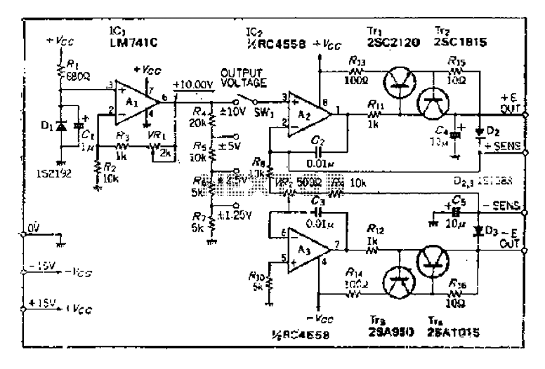
The maximum input voltage is 10V. An operational amplifier (op-amp) is used to provide a reference voltage of 10V, with its stability primarily determined by the characteristics of a temperature-compensated Zener diode (IS2192). The Zener voltage (Vz) can be...
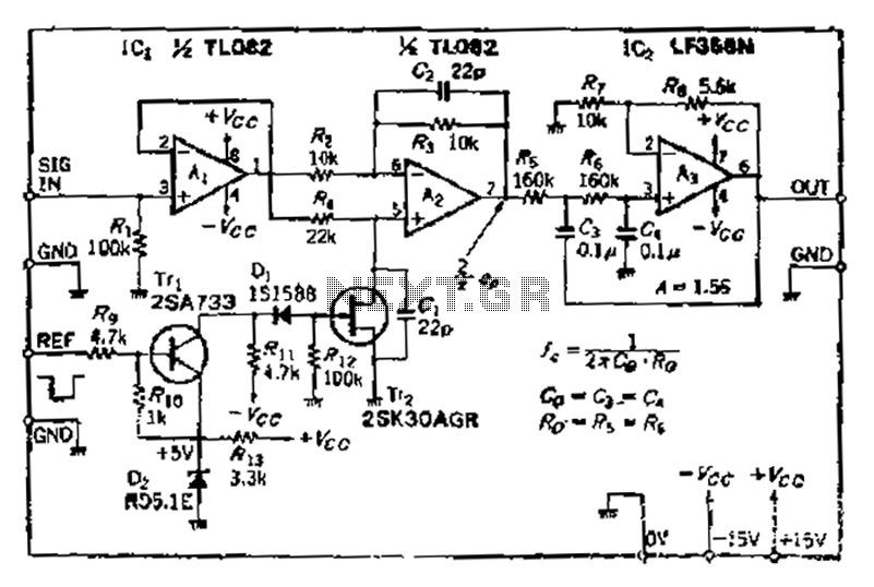
After turning off TT2, the input signal enters through chi Az, where the input resistance is very high and reaches the same potential. The inverting input terminal must also be associated with this movement. Therefore, Trr functions as a...
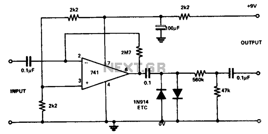
The circuit utilizes the 741 operational amplifier, which has a maximum gain of 20,000. However, the design achieves a gain of 2.7 million, resulting in output distortion. This distortion is attributed to noise effects. Two clamping diodes are employed...
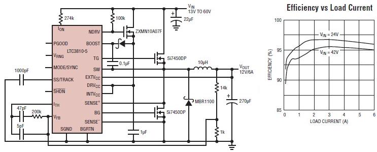
The LTC3810-5 synchronous step-down switching regulator controller allows for the design of a straightforward 12-volt switching power supply electronic project with minimal external components. This controller can directly reduce voltages from up to 60V, making it suitable for telecommunications...
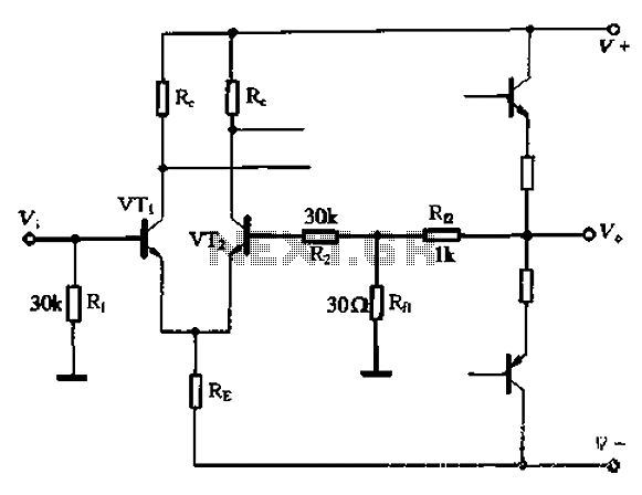
The circuit utilizes the configuration illustrated in Figure 1-36, with the feedback circuit and bias circuit implemented separately. The feedback resistor, Rfl, is approximately 30 ohms. To maintain the desired amplification, the resistor R queue is set to 1...
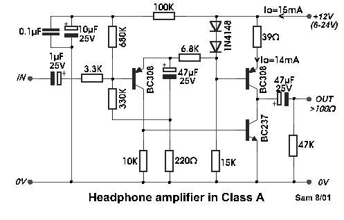
Even if the circuit is simple, it complies with all conditions regarding distortion and frequency response. The input resistance is 250K ohms, and it can drive loads ranging from 100 ohms to 2K ohms. The described circuit is a fundamental...