
1880MHz internal bias circuit diagram of the amplifier application collector RF2324

The RF2324 amplifier circuit operates at a frequency of 1880MHz, primarily used in wireless communication applications. The RF signal enters through pin 3, where it is initially amplified by a preamplifier stage. This preamplification is crucial for enhancing the weak RF signals to a level suitable for further processing. The term "7 feet" refers to the distance or the layout of the circuit traces, which can influence the signal integrity and performance due to parasitic capacitance and inductance.
The internal amplifier is coupled with a 10pF capacitor, which is strategically placed to block any DC components while allowing the RF signal to pass through. This coupling capacitor is essential in maintaining the desired signal characteristics while preventing DC bias from affecting the amplifier's operation. Impedance matching at 50 ohms is critical in RF circuits to minimize signal reflections and maximize power transfer, which is achieved through careful design of the external output matching network.
The open collector output terminal, referred to as "7 feet," can connect to a power supply (Vcc) through either a choke or a matching inductor. This connection aids in stabilizing the voltage supply and filtering out unwanted noise. The external output matching network is designed to ensure that the amplifier's output impedance aligns with the system's requirements, optimizing both output power and efficiency.
The power-down control terminal, indicated as "1 foot," allows for the circuit to be turned off when not in use, thereby conserving power. The specified voltage levels for VPD are critical for the operation of the circuit; a voltage of 2.8V ± 0.1V keeps the circuit active, while a drop to 0.9V effectively disables it. The need for an additional RF bypass circuit for VPD indicates that further filtering may be necessary to ensure stable operation and prevent unwanted oscillations or noise from affecting the amplifier's performance. Overall, this circuit design exemplifies careful consideration of RF principles to achieve reliable and efficient amplification in communication systems. As shown in FIG constituted by RF2324 1880MHz internal amplifier collector bias application circuit. Radio frequency (RF) signal from the input pin 3, via a preamplifier, after the last stage power amplifier output is amplified by 7 feet. 3 feet directly coupled to the internal amplifier, thus blocking plus a 10pF of capacitance coupling, impedance matching at 1880MHz work to 50. 7 feet for the open collector output terminal can be connected to the power supply Vcc through choke or matching inductor, the pin impedance matching is typically 50, external output matching network allows the amplifier output impedance matching for maximum output power and efficiency.
1 foot for the power down control terminal. When VPD 2.8V 0.1V when (IPD is typically 8.5mA) circuit; when VPD 0.9V circuit closes. VPD requested additional RF bypass circuit.
Related Circuits
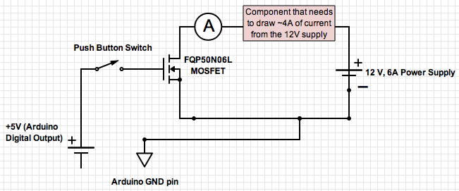
If the ground of the Arduino is disconnected from the negative terminal of the power supply, current flows through the MOSFET, even when the switch is not closed. In an electronic circuit involving an Arduino and a MOSFET, maintaining a...

A compact, inexpensive and low component count telecom headset can be constructed using two readily available transistors and a few other electronic components. This circuit is very useful for hands-free operation of EPABX and pager communication. Since the circuit...
This 1500W Power Amplifier Circuit Diagram contains two images of the circuit. For more complete information, refer to the main post titled "1500 Watt Power Amplifier." It includes a list of component parts for the 1500W Power Amplifier Circuit...
This article explains the principle of the Audison LR604XR amplifier. The principle is straightforward; it is recommended to combine the text with a careful reading of the complete schematic. To fully understand this principle, it is advisable to review...
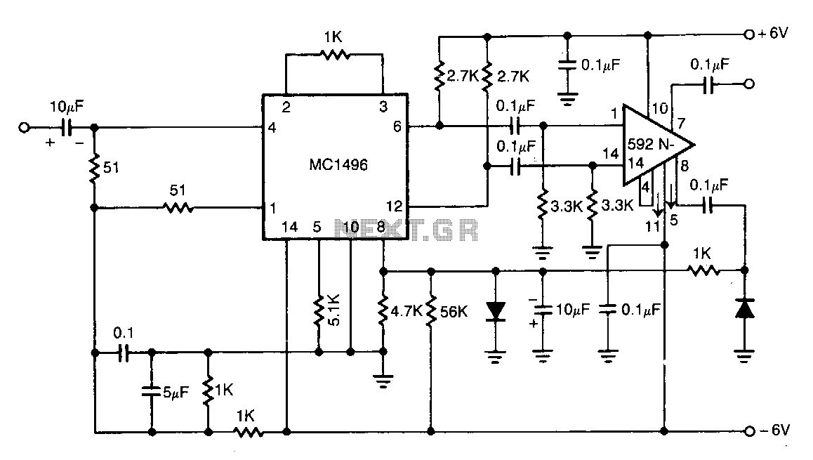
The NE592 is connected with the MC1496 balanced modulator to create an effective automatic gain control system. The signal is input to the MC1496 and then re-coupled to the NE592. Unbalancing the carrier input of the MC1496 allows the...
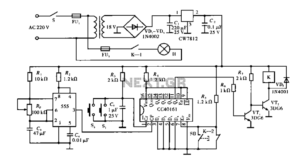
Corridor counter delay circuit for controlling lights. This circuit is tested and functional. When the circuit is energized, the 555 oscillator starts to oscillate. The CC40161 is cleared, and an integrating circuit composed of R3 and C5 transitions the...