
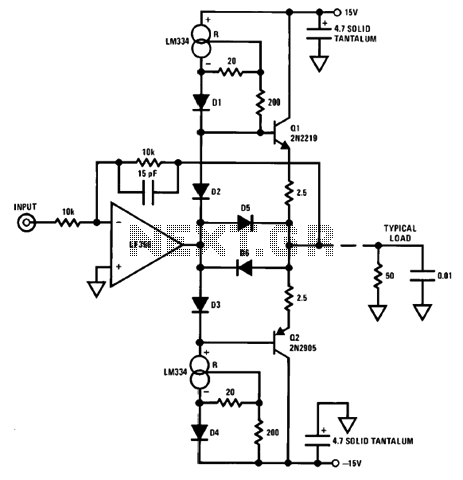
200mA 12V Op Current Gain Stage
An output booster circuit is essential in applications where the signal needs to be amplified to meet specific current or voltage requirements. This circuit typically consists of a transistor-based configuration, which can be either a bipolar junction transistor (BJT) or a field-effect transistor (FET), depending on the desired characteristics and performance.
The fundamental purpose of the output booster is to enhance the output power while ensuring that the dynamic response of the system remains optimal. This is particularly important in scenarios where the load demands exceed the capabilities of the driving IC. The design includes feedback mechanisms to stabilize the gain and reduce distortion, which is crucial for maintaining signal integrity.
In a typical current gain stage, the input signal is fed into the base (or gate) of the transistor, which controls the flow of current from the collector (or drain) to the emitter (or source). The configuration can be set up in common emitter (or common source) mode to provide significant voltage gain, or in common collector (or common drain) mode to deliver high current gain with low output impedance.
The circuit may also incorporate additional components such as resistors for biasing, capacitors for coupling and bypassing, and inductors for filtering, which collectively aid in achieving the desired frequency response and stability. Careful selection of these components is necessary to optimize performance for specific applications, ensuring that the booster can handle the required power levels without introducing excessive noise or distortion.
Overall, the design of an output booster circuit is a critical aspect of electronic system design, particularly in high-performance applications where power efficiency and signal fidelity are paramount.An output booster is needed when you want to achieve the needed current/voltage gain. Great output commonly need in accociation with the the output power limitation of mostly IC processing. The following figure shows you circuit diagram of the typical current gain stage if you want to design a booster stages which achieve power gain while maintaining good dynamic performance.
The design of. 🔗 External reference
Related Circuits

A simple but effective fixed gain transformerless microphone preamplifier circuit diagram is shown in the picture below. The circuit amplifies differential signals from low impedance microphones by 50 dB and has an input impedance of 2 kOhms. The OP27/37...
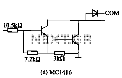
The MC1411 series features a Darlington drive current internal structure that offers small, consistent, and highly reliable parameters. This series is particularly effective for high-voltage applications and can directly drive loads such as relays and lights. It includes wheeling...

The bi-directional sequencer employs a 4-bit binary up/down counter (CD4516) along with two "1 of 8 line decoders" (74HC138 or 74HCT138) to create the well-known "Night Rider" display. A Schmitt Trigger oscillator generates the clock signal for the counter,...

A current loop transmitter refers to a sensor system utilized in industrial 4-20mA current loop technology. This transmitter contains the... A current loop transmitter is a critical component in industrial automation and control systems, particularly in applications where analog signal...
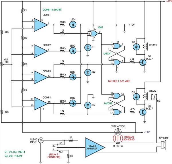
This circuit utilizes a 0.1Ω 1W resistor connected in series with the output of a power amplifier. When the amplifier delivers 100W into an 8Ω load, the resistor dissipates 1.25W. The temperature rise is detected by a thermistor thermally...
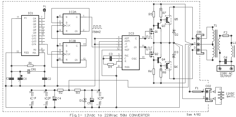
In many situations, there is a need for a 220VAC voltage supply in areas where it is not readily available to power various small appliances. Figure 1 illustrates a voltage converter circuit that converts 12VDC to 220VAC, with an...