
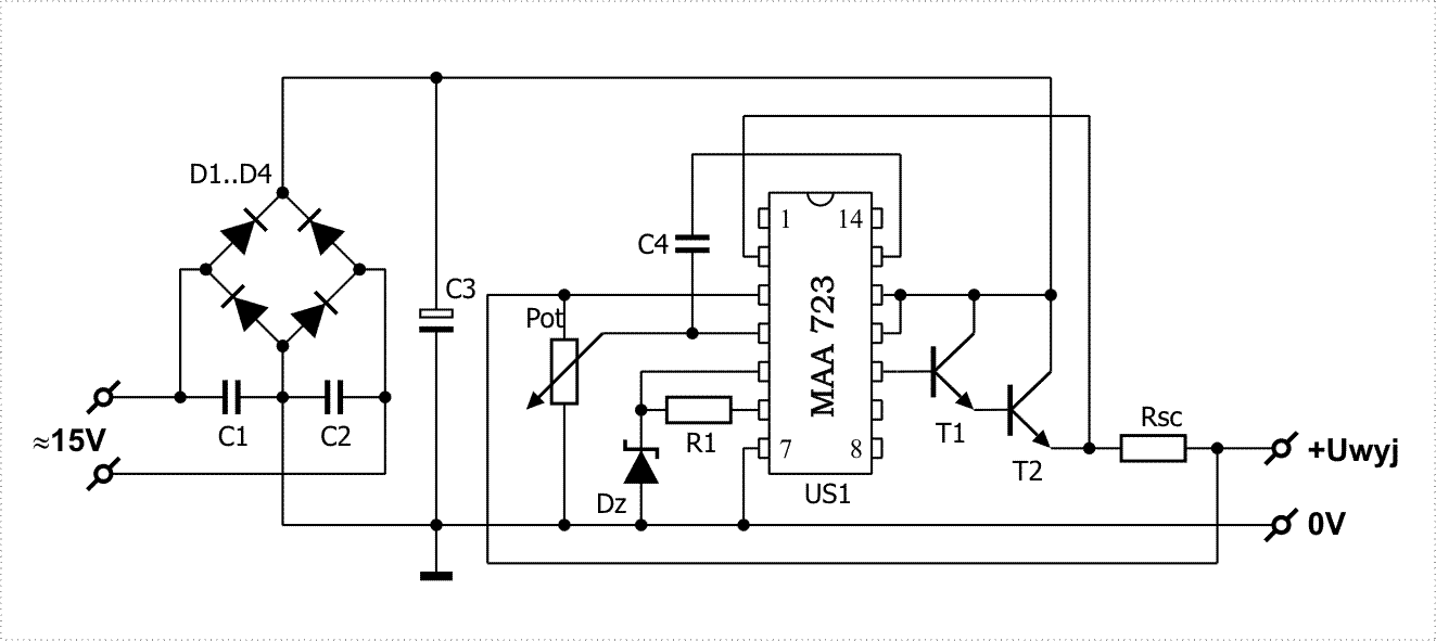
200W ATX PC POWER SUPPLY

The power supply circuit described operates using a combination of analog control and feedback mechanisms to regulate output voltages effectively. The TL494 chip serves as a PWM controller, providing precise regulation of the output voltages while ensuring stability under varying load conditions. The push-pull configuration of the transistors allows for efficient switching and minimizes energy loss during operation.
The input filter circuit, consisting of capacitors, resistors, and transformers, serves to smooth out the incoming AC voltage, reducing ripple and noise before it reaches the rectifier. The rectification process converts AC voltage to DC, and the subsequent filtering ensures that the output is stable and free of fluctuations.
Overvoltage protection is critical in safeguarding the power supply and connected components. The varistors Z1 and Z2 act as clamping devices, diverting excess voltage away from sensitive components. The thermistor NTCR1 plays a vital role in inrush current limiting, preventing damage during initial power-up.
The feedback loop established by resistors R25 and R26 allows the control chip IC1 to monitor output voltages continuously and make necessary adjustments to maintain regulation. The design ensures that even during transient conditions, the output remains stable, providing reliable power to the motherboard and peripherals.
In summary, this power supply design exemplifies standard practices in modern power supply engineering, incorporating features such as voltage regulation, protection mechanisms, and efficient switching techniques to deliver stable and reliable power to electronic devices.I bring you wiring diagram of PCs power supply of DTK company. This power supply has ATX design and 200W performance. I was drawed diagram, when I repaired this power supply. This power supply circuit uses chip TL494. Similar circuit is used in the most power supplies with output power about 200W. Device use push-pull transistor circuit with regulation of output voltage. Line voltage goes through input filter circuit (C1, R1, T1, C4, T5) to the bridge rectifier. When voltage is switched from 230V to 115V, then rectifier works like a doubler. Varistors Z1 and Z2 have overvoltage protect function on the line input. Thermistor NTCR1 limits input current until capacitors C5 and C6 are charged. R2 and R3 are only for discharge capacitors after disconnecting power supply. When power supply is connected to the line voltage, then at first are charged capacitors C5 and C6 together for about 300V. Then take a run secondary power supply controlled by transistor Q12 and on his output will be voltage.
Behind the voltage regulator IC3 will be voltage 5V, which goes in to the motherboard and it is necessary for turn-on logic and for "Wake on something" functions. Next unstabilized voltage goes through diode D30 to the main control chip IC1 and control transistors Q3 and Q4.
When main power supply is running, then this voltage goes from +12V output through diode D. In stand-by mode is main power supply blocked by positive voltage on the PS-ON pin through resistor R23 from secondary power supply. Because of this voltage is opened transistor Q10, which opens Q1, which applies reference voltage +5V from pin 14 IO1 to pin 4 IO1.
Switched circuit is totally blocked. Tranzistors Q3 and Q4 are both opened and short-circuit winding of auxiliary transformer T2. Due to short-circuit is no voltage on the power circuit. By voltage on pin 4 we can drive maximum pulse-width on the IO1 output. Zero voltage means the highest pulse-width. +5V means that pulse disappear. Somebody pushes the power button on computer. Motherboard logic put to ground input pin PS-ON. Transistor Q10 closes and next Q1 closes. Capacitor C15 begins his charging through R15 and on the pin 4 IC1 begins decrease voltage to zero thanks to R17. Due to this voltage is maximum pulse-width continuosly increased and main power supply smoothly goes run.
In a normal operation is power supply controlled by IC1. When transistors Q1 and Q2 are closed, then Q3 and Q4 are opened. When we want to open one from power transistors (Q1, Q2), then we have to close his exciting transistor (Q3, Q4). Current goes via R46 and D14 and one winding T2. This current excite voltage on base of power transistor and due to positive feedback transistor goes quickly to saturation.
When the impulse is finished, then both exciting transistors goes to open. Positive feedback dissapears and overshoot on the exciting winding quickly closes power transistor. After it is process repetead with second transistor. Transistors Q1 and Q2 alternately connects one end of primary winding to positive or negative voltage. Power branch goes from emitor of Q1 (collector Q2) through the third winding of exciting transformer T2.
Next throug primary winding of main transformer T3 and capacitor C7 to the virtual center of supply voltage. Output voltages +5V and +12V are measured by R25 and R26 and their output goes to the IC1. Other voltages are not stabilised and they are justified by winding number and diode polarity. On the output is necessary reactance coil due to high frequency interference. This voltage is rated from voltage before coil, pulse-width and duration cycle. On the output behind the rectifier diodes is a common coil for all voltages. When we keep direction of windings and winding number corresponding to output voltages, then coil works like a transformer and we have compensation for irregular load of individual voltages.
In a common practise are voltage de 🔗 External reference
Related Circuits
The objective is to enhance information transmission through the distribution of articles. Please contact us via email at [email protected] within 15 days if there are any issues related to article content, copyright, or other concerns. Prompt action will be...
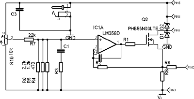
This is the first version of a laser diode power supply and current source using an n-channel power device. Components include LM358D IC, transistor, resistor, and others. The described circuit functions as a power supply specifically designed for laser diodes,...
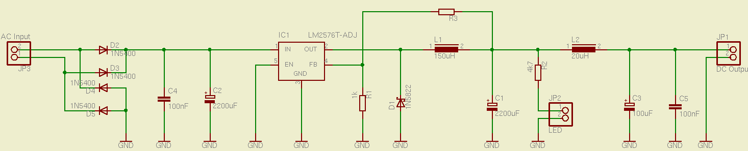
This is a simple and effective switched mode power supply (SMPS) designed to power an LCD monitor. It requires 20V at 2.3A, but the power supply unit (PSU) output voltage can be adjusted in the range of 1.2V to...

High voltage resistors for the high voltage divider are SFERNICE or PHILIPS type VR37 (3.5 kV - 0.4 W). They are not expensive (even if they are sold in quantities of 25 or 50 units), and it is always...
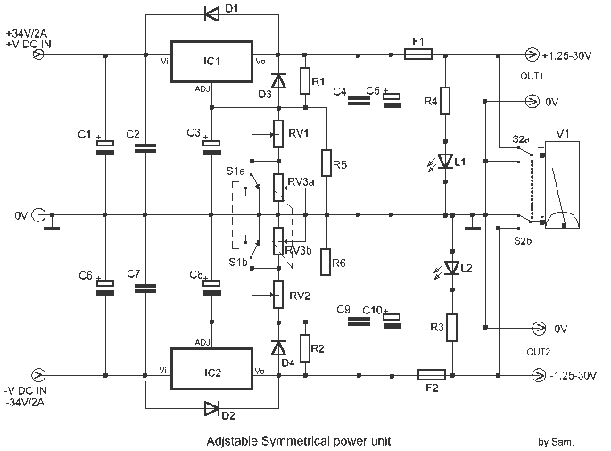
This is the voltage converter to get the voltage of ±1.25-30V from the input voltage of ±35V. I am using the 3 terminal voltage regulator for the voltage to be changed in this unit. As the regulator, LM317 is...
When the power is turned off, the alarm activates when switch S1 is closed. The 12-V battery remains charged when the circuit is connected and the switch is in the "on" position. The described circuit features an alarm system that...