
24v to 16v circuit diagram of a buck

The LT1934 chip is designed to deliver high efficiency and reliability in power supply applications, making it suitable for various electronic devices. The integration of a reference voltage source and an error amplifier allows for precise voltage regulation, which is essential in maintaining stable output under varying load conditions. The PWM control mechanism employed in the LT1934 enables efficient conversion of higher input voltages to lower output voltages, which is particularly beneficial in battery-operated devices where power conservation is critical.
In the implementation of the LT1934 circuit, careful attention to the selection of passive components is paramount. The choice of the inductor (L1) directly influences the performance characteristics of the power supply. An inductor with appropriate inductance value ensures optimal energy transfer during the switching cycles, minimizing losses. Inductors must be selected based on their saturation current ratings to prevent performance degradation under load.
Furthermore, the layout of the PCB plays a significant role in the overall performance of the LT1934 circuit. It is recommended to minimize the distance between the LT1934 chip and its associated capacitors to reduce parasitic inductance and resistance, which can adversely affect the stability and efficiency of the circuit. Utilizing a ground plane can enhance the return path for high-frequency currents, further improving performance and reducing noise susceptibility.
In summary, the LT1934 chip offers a versatile solution for efficient DC/DC conversion, with design considerations that prioritize component selection and PCB layout to achieve optimal performance. As shown program uses Linears LT1934 chip production, high cost, high overall efficiency of the electricity load circuit design is less demanding, there are a lot of adjustment margin. When input 24VDC, the input is not isolated a set of output 5V, 9mA current, and input isolation of a set of output 5V, 4mA current, 24VDC bus current can easily do less than 3.5mA, efficiency can reach 85%. LT1934 series chip is a reference voltage source, an oscillation circuit, and the like of the error amplifier, CMOS step-down DC PWM control/DC controller.
Key indicators: input voltage 3.3~34V, the output voltage is 1.5~6.0V, 0.1V can be set for the advanced units; low quiescent current of 12 A maximum, maximum output current 300mA. Figure 4 is a basic circuit LT1934. In the design of the circuit, component selection and S-8251 is basically the same in PCB layout design should pay attention LT1934 chip capacitors C2 and distance can not be too far away, try to use thick lines, it is best to use a ground plane, otherwise it will lead to self-oscillation.
Inductor L1 for DC/DC conversion efficiency play a decisive role. If L1 is too small, the conversion efficiency of the circuit will be reduced starting current is increased, can not even start. If L1 is too large, it may cause decreased output capacity, while the DC/DC circuit may oscillate.
Related Circuits
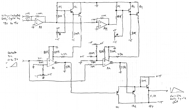
A discussion took place on synth-diy regarding the challenges of constructing a voltage-controlled oscillator with a sawtooth wave output, where the duty cycle (the ratio of ramp-up time to ramp-down time) can be adjusted using a separate control voltage....
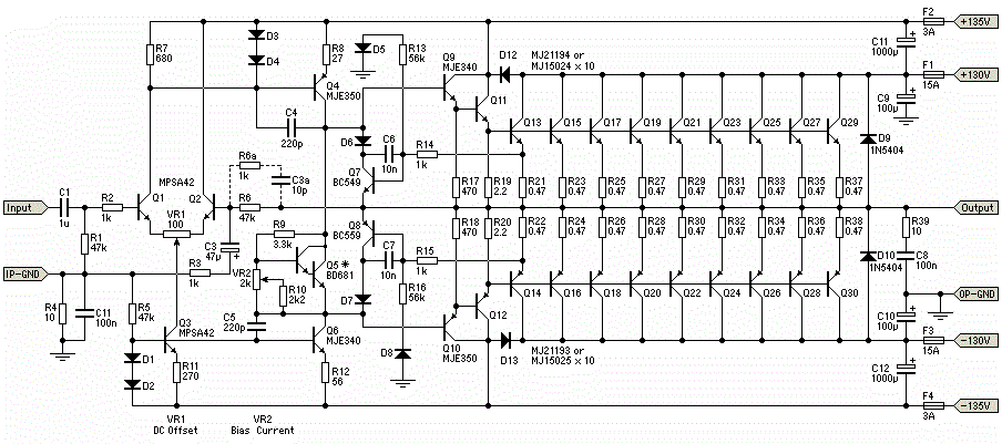
The circuit for the power amplifier has a power output of up to 1500W RMS and is commonly utilized in outdoor sound systems. The final image displays a series of power amplifiers that utilize 10 sets of power transistors....
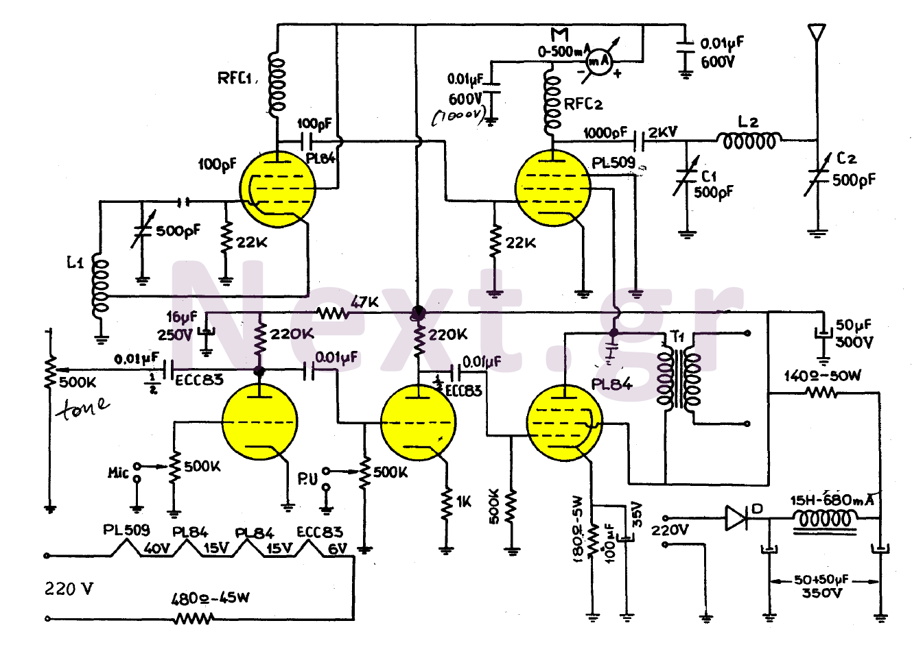
The simplicity of this transmitter, combined with its high performance, makes it particularly interesting. It has an output power of approximately 30 W, and under normal conditions, with the appropriate antenna and handling, it can achieve a range of...
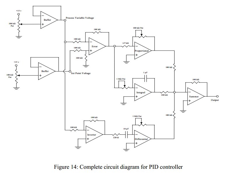
Convert a feedforward operational amplifier PID loop to C code. Assistance is needed for this conversion, as the process is unfamiliar. Input values can be obtained through an ADC, such as voltage or current, but coding a feedforward PID...
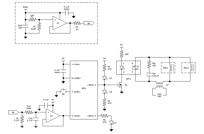
While discussing an all-linear automatic night light circuit, it was mentioned that an MCU-based Automatic Night Light Controller (ANLC) was being tested. The firmware has been tweaked since then. Recently, the sensor was installed outdoors and connected to control...
This circuit measures the distance covered during a walk. The hardware is located in a small box that can be slipped into a pants pocket. The display is designed such that the leftmost display, D2 (the most significant digit),...