
Voltage Controlled Duty Cycle Sawtooth Circuit

This circuit schematic outlines a voltage-controlled oscillator designed for synthesizer applications, specifically targeting the generation of adjustable duty cycle sawtooth waveforms. The use of CA3280 OTAs allows for precise control over the output characteristics, leveraging their transconductance properties to achieve the desired gain adjustments. The incorporation of LF412 op-amps ensures low noise and high-speed operation, which is critical in audio frequency applications.
The design emphasizes the importance of maintaining a consistent output amplitude while varying the duty cycle, which can significantly impact the harmonic content of the generated waveform. By utilizing exponential circuits to manage the gains, the circuit can achieve a smooth transition between different duty cycles, enhancing the musicality of the output.
Moreover, the emitter follower configuration employed by transistors Q5 and Q6 serves to buffer the output, thus preserving signal integrity while allowing for the necessary voltage level adjustments. The careful selection of resistor values throughout the circuit ensures optimal performance, addressing both input and feedback paths to maintain stability and linearity in the oscillator's response.
Overall, this schematic serves as a robust foundation for synthesizer enthusiasts and engineers looking to explore the creative possibilities of voltage-controlled oscillators with adjustable duty cycles, facilitating innovative sound design and musical expression.There was a discussion on synth-diy a while ago about the problems of building a voltage controlled oscillator with a sawtooth wave output whose duty cycle (the ratio of ramp-up time to ramp-down time) is adjustable with a seperate control voltage. [Don: When you get around to it, talk about the musical advantages of such a thing, morphing, the ha rmonic spectra, the way to build a potentiometer controlled variable duty cycle oscillator, why you can`t just integrate a PWM square wave, and so forth. ] In the following schematic, the input on the left is an audio frequency rising sawtooth wave going from 0.
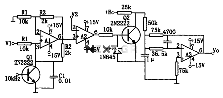
0V to +5. 0V. The input on the upper left is a duty cycle control voltage going from -5. 0V (falling sawtooth) through 0. 0V (triangle wave) to +5. 0V (rising sawtooth). The power supply is +/- 15. 0V. A1 and A2 are CA3280 OTAs. A3 and A4 are LF412 op amps. The transistors are reasonable high beta NPNs and PNPs. The values for the trimming circuitry is intentionally left off. The basic idea is to take our rising sawtooth source and it`s inverse, a falling sawtooth from +5. 0V to 0. 0V, adjust the relative gains of those two, and use the arithmetic minimum of those two signals as the output. The gains would ideally go from 1. 0 to infinity, but for practical reasons I`ve limited the range to 1. 11 through 10. If the two gains are equal to 2. 0 the output will be a triangle wave. To keep the output amplitude constant the two gains should be such that the sum of the recipricals of the gains is constant.
And if the output amplitude is going to be the same as the input amplitude, that constant value needs to be unity. For this application, x is proportional to the duty cycle control voltage, centered around zero for a 50% duty cycle.
1+ex is proportional to one of the gains and 1+e-x is proportional to the other. The ex and e-x are implemented with simple ARP-style exponential circuits, and the 1s in the denominators are currents from resistors. The signal path starts with the given sawtooth wave. A1 and A2 are set up run at 0. 24 mA for a 50% duty cycle; we need plenty of headroom to increase this gain, but the current for the lowest gain still needs to drive the output to full amplitude.
The 82k resistors set the OTAs` input diode current to 170uA, for a diode resistance of 416 ohms, for an input attenuation of 1/100th, easily accomodating the input amplitude. From here, an OTA bias current of 0. 24mA (triangle wave) and the 51k ohm output resistor will set the total gain to 2. 0. Transistors Q5 and Q6 are emitter followers with the lowest voltage taking over. The output emitter follower compensates for the offset voltage of the previous transistor two. Not exactly, but close enough for now. Op amp A3 creates mixes the input control voltages, op amp A4 provides the negative. Both of these go to the ARP-style exponential circuits. Adjust them to idle at 0. 12mA each. The 120kohm resistors are responsible for the 1s in the denominators of the equation and the 4. 7kohm resistors limit the control current into the OTAs to a reasonble value. Correction: The resistor values on the inputs of A2 are wrong. They should be, top to bottom, 62k, 39k, and 20k. They are supposed to bias A2`s input so the sawtooth effectively ramps down from 5. 0 volts. 🔗 External reference
Related Circuits
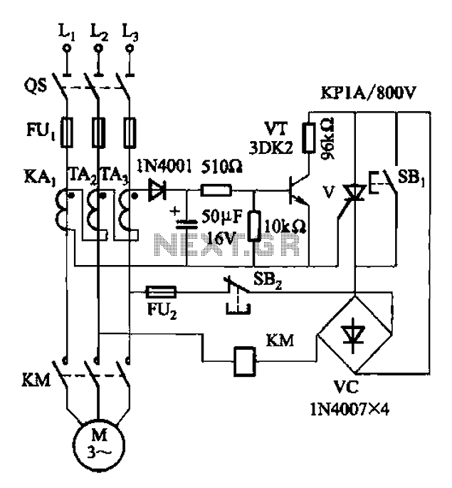
Both circuits are used to control the thyristor contactor KM action to overcome the break phase protection relay prone to malfunction or refuse to move, and enhance the sensitivity and reliability of the protection device. The described circuits are designed...
As illustrated in the dividing circuit diagram, A1 consists of a voltage-controlled current source, A2 functions as a voltage comparator, and A3 is configured as an active low-pass filter. When the time constant R1C1 is equal to the clock...
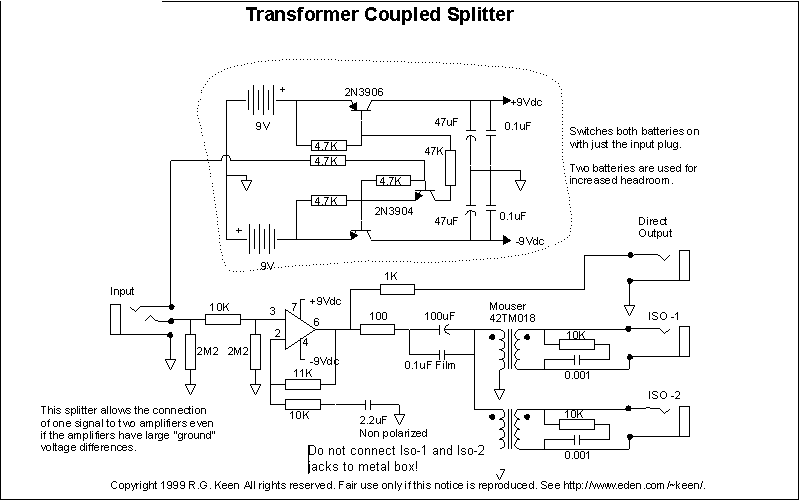
An active amplified transformer isolated signal splitter that enables a hum-free connection of one guitar to multiple amplifiers, while also providing a direct output. This includes a discussion on using audio transformers for equipment interconnections and mentions line-level transformers...
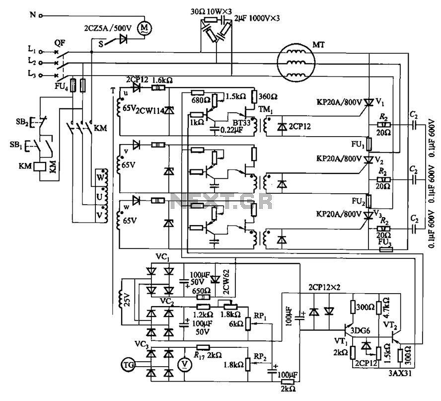
The circuit depicted in Figure 3-181 comprises three thyristors, labeled V1 to V3. The trigger circuit utilizes a single-junction transistor relaxation oscillator. The speed control circuit incorporates negative feedback. A master adjust potentiometer, designated as RPi, is used to...
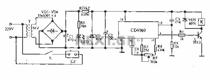
A CD4060 production time controller circuit is illustrated below. It is connected in such a way that R5 and C3 form a differential circuit to create a delay time from the start. Under the influence of the oscillating signal,...
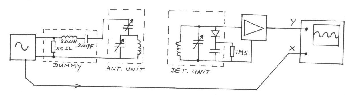
The frequency remains constant, oscillating between two predetermined values. On the oscilloscope display, a frequency spectrum is observed, showcasing the response curves of the two circuits. The input voltage of the receiver is 0.1 Volt peak-to-peak, while the voltage...