
2N2222 Crystal Oscillator

This crystal oscillator circuit utilizes a fundamental crystal to generate a stable sinewave output with minimal distortion and phase noise. The design is optimized for low power consumption, specifically aiming for less than 1 mW of power dissipation in the crystal itself. The crystal acts as a frequency-selective element, filtering the signal current and developing a corresponding voltage across a capacitor, which is characterized by a reactance of approximately 500 ohms.
The inclusion of a JFET (Junction Field Effect Transistor) buffer stage is a critical design feature, as it allows the oscillator to effectively drive lower impedance loads without significant signal degradation. This buffer stage ensures that the output can maintain its integrity when interfacing with subsequent circuit components.
To further enhance the circuit's capability to drive loads with a characteristic impedance of 50 ohms, additional buffering is recommended. This can be achieved through the implementation of an emitter follower configuration, which provides high input impedance and low output impedance. Additionally, a voltage step-down transformer or a matching network may be employed to ensure optimal power transfer and signal fidelity.
Component C3, which is part of the output network, can be adjusted to optimize the output voltage level. Reducing C3 may increase the output voltage or allow for lower drive levels, whereas increasing its value may be beneficial for achieving lower output levels.
In cases where overtone crystals are utilized, the standard 1k ohm emitter resistor can be replaced with an appropriately selected choke. This choke should be chosen to resonate with capacitor C2, thereby enhancing the circuit's performance at the overtone frequency. This adjustment allows for better matching and efficiency in the oscillator's operation, ensuring that the output remains stable and within desired operational parameters.This crystal oscillator is designed to operate with fundamental crystals with less than 1 mW dissipated in the crystal. The signal current is filtered by the crystal and develops a voltage across a capacitor with about 500 ohm of reactance.
The resulting sinewave has low distortion and phase noise. A JFET buffer is included to drive lower impedance loads. Further buffering with an emitter follower and a voltage step-down transformer or matching network is recommended for driving 50 ohm loads. C3 may be reduced for larger output voltage or to allow lower drive level or it may be increased when lower output levels are desired. The 1k emitter resistor may be replaced with a choke when using overtone crystals. Select the choke to resonate with C2 🔗 External reference
Related Circuits
.jpg)
Integrated circuits (ICs) with on-board oscillators that require low-frequency fundamental crystals are common; however, IC frequency multipliers now require the higher frequencies provided by third overtone crystals. The third-overtone (3OT) crystal oscillator is more complex than its fundamental counterpart,...
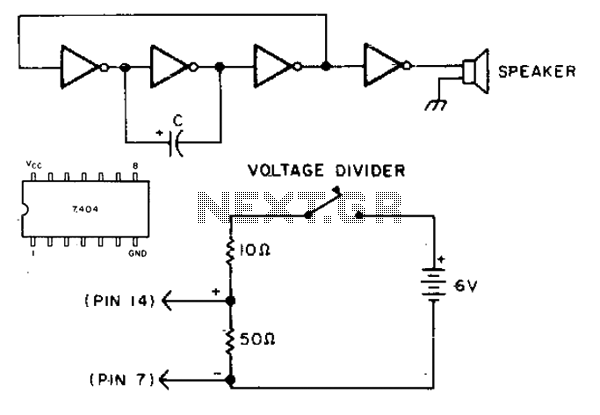
This simple circuit utilizes the 7404 low-power Schottky hex inverter. Capacitor C is a 5 to 30 µF electrolytic capacitor selected for the desired pitch. The speaker is a 2-inch, 8-ohm unit. The circuit employs a 7404 low-power Schottky hex...
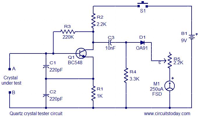
This is a straightforward and cost-effective circuit designed for testing quartz crystals. A Colpitts oscillator is employed using transistor T1. When the crystal is connected between terminals A and B, the circuit generates high-frequency oscillations. These oscillations will only...
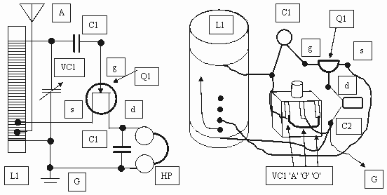
The source connection is tapped into the tuning coil low down, as a means of impedance matching with the headphones and acts as the anode, while the drain connects with your headphones as the cathode, to complete the detector...
This circuit operates at 36V with a current of 500mA on the front side, while it features a 36V charging capability on the back side. The brightness is comparable to that of a 240V light bulb, considering it is...
Switchable Output Crystal Oscillator Circuit. This oscillator circuit allows crystals to be electronically switched using logic commands. The circuit is best understood by initially ignoring all crystals. Furthermore, assume that a... The switchable output crystal oscillator circuit is designed to...