
3.3V and 5V DC DC converter circuit design using LT3692 DC converter dual tracking regulator

The LT3692 is an advanced solution for applications requiring efficient power conversion with minimal component count. This dual-channel DC-DC converter is designed to operate in a variety of environments, making it suitable for both consumer electronics and automotive applications. The independent input voltage feature allows for versatility in power sourcing, enabling the converter to adapt to different voltage levels as needed.
The programmable maximum current limit is a critical feature that allows designers to set the output current to match the specific requirements of the load, thereby preventing overcurrent conditions that could damage the circuit. The synchronization capability, whether through an external clock or an internal oscillator, ensures that multiple converters can operate in harmony, reducing electromagnetic interference and enhancing overall system performance.
The 180° phase relationship between the two channels is particularly beneficial in applications where minimizing output voltage ripple is essential. This design choice allows for smoother operation and improved transient response, which is crucial in applications where load conditions may change rapidly.
The output voltage tracking feature provides flexibility in applications where the output voltage needs to be adjusted dynamically based on the load or system requirements. This capability is particularly useful in battery management systems and other power-sensitive applications.
The enhanced short-circuit protection ensures that the converter can withstand fault conditions without sustaining damage, thereby increasing the reliability of the overall system. The low dropout capability allows for efficient operation even when the input voltage is close to the output voltage, maximizing the utility of the available power supply.
Finally, the low shutdown current is advantageous for battery-powered applications, as it helps extend battery life by minimizing power consumption during idle periods. Overall, the LT3692 dual current mode PWM step-down DC-DC converter represents a robust and flexible solution for a wide range of electronic power supply needs.Using the LT3692 dual current mode PWM step-down DC DC converter circuit with two internal 3. 5A switches can be designed a very simple power supply circuit, that can be used for various electronic circuits applications like : distributed supply regulations or automotive circuits. LT3692 provide independent input voltage, shutdown, feedback, soft -start, current limit and comparator pins for each channel. To optimize efficiency and component size, both converters have a programmable maximum current limit and are synchronized to either a common external clock input, or a resistor settable fixed 250kHz to 2. 25MHz internal oscillator. A frequency divider is provided for channel 1 to further optimize component size. At all frequencies, a 180 ° phase relationship between channels is maintained, reducing voltage ripple and component size.
A clock output is available for synchronizing multiple regulators. This DC DC converter circuit presented in this schematic diagram, will provide two independent voltages :3. 3 volts and 5 volt. The maximum output current that can be provided by this DC DC converter electronic project is around 3A for each channel.
As you can see in this schematic circuit, this project require few external electronic parts and needs to be powered from a 12 volt DC power supply. Some features of this DC DC converter electronic project are : independent synchronized switching frequencies, antiphase switching, flexible output voltage tracking, enhanced short-circuit protection, low dropout: 95% maximum duty cycle, low shutdown current: <10 A.
🔗 External reference
Related Circuits
This circuit is representative of the typical application of a photomultiplier tube. The circuit depicted is AC coupled; however, if DC coupling is required, the capacitor can be removed, and an appropriate interfacing method should be employed. A common...
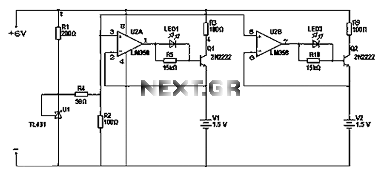
There are two differing opinions regarding the charging of alkaline batteries. Some assert that charging is effective, while others caution against it due to the risk of explosion. It is acknowledged that rechargeable alkaline batteries can typically endure 30...
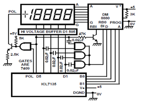
A circuit diagram for driving a plasma-type display using the ICL7135 is presented in the schematic. This application highlights the versatility of this integrated Analog to Digital Converter device. The ICL7135 is a high-precision, low-power, integrating Analog to Digital Converter...
The market offers numerous devices that replace traditional wall switches, allowing for the adjustment of bulb luminosity. For those looking to create an "intelligent" home or a more complex device for controlling light bulb power, several options are available....
Here is a design circuit for a frequency modulator that is equipped with a tuning circuit. In this circuit, a pair of 1N4007 diodes is utilized as varactor diodes. The choice of 1N4007 diodes is not due to their...

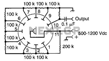
The current generated flows through clips placed on the earlobes. The output current is adjustable from 80 to 600 microamperes, following the recent launch in Europe. The described device utilizes a current generation mechanism that delivers a controlled microcurrent through...