
4-input mini Logic Analyzer
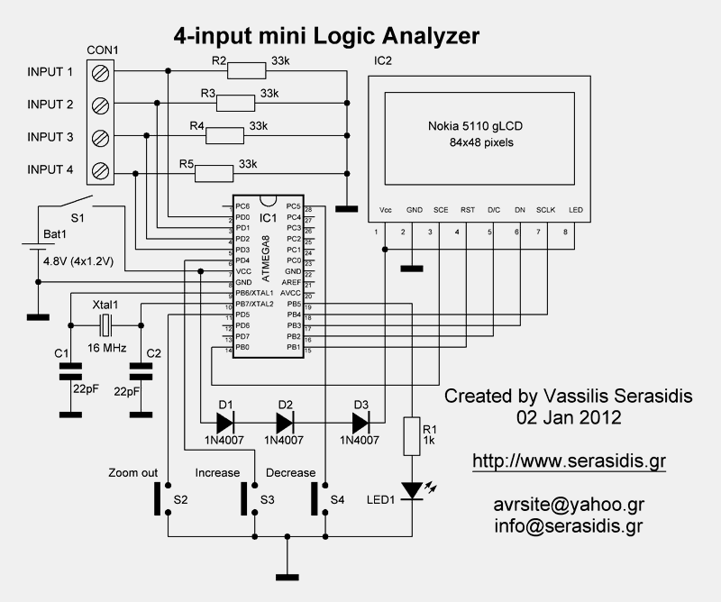
The mini logic analyzer circuit is designed to provide a user-friendly interface for monitoring digital signals, making it an invaluable tool for electronics engineers and hobbyists alike. The core of the circuit is based on a microcontroller (AVR), which handles signal processing and data storage. The choice of using pull-down resistors ensures that the inputs remain stable, mitigating the risk of false triggering from stray signals. The LCD display serves as a critical component, providing real-time feedback on the signal transitions, while the voltage regulation via diodes ensures that the display operates within safe limits.
In terms of data handling, the internal RAM buffer is a crucial feature, allowing for the temporary storage of signal data before it is visualized. The design considerations for the buffer size reflect a balance between memory usage and capturing speed, which is essential for accurate signal analysis. The ability to adjust the zoom level of the displayed graph enhances usability, enabling users to focus on specific segments of the signal over varying time scales.
The incorporation of rechargeable batteries not only makes the device portable but also environmentally friendly, as it reduces waste from disposable batteries. Overall, this mini logic analyzer circuit exemplifies an efficient and practical approach to digital signal analysis, suitable for a wide range of applications in electronics.This mini Logic analyzer is a tool for you to watch on LCD the logic transitions 0 or 1 of a digital data signal. A digital data signal can be found on the output pin of TSOP-1730 Infrared Receiver, on the Transmit and reveive pins of MAX-232 chip (RS-232), on Clock and Data pins of I2C data bus and many more electronic components.
This circuit su pports capturing forup to 100 kHz digital signals. The operating voltage of the circuit is 4. 8V DC from 4x1. 2V rechargeable batteries. Switch on the S1 to power on the electronic circuit. After the initial screens on LCD you will see a message that the AVR waits for a signal change on input pins. The AVR has 4 external pull-down resistors 33kG™ (R2-R5) avoiding any unnecessary trigger on any input pin because of an external electromagnetic field or by touching accidentally your hand on any input pin.
The Nokia 3310/5110 LCD works from 3. 3 - 5V power supply. The problem is that the LCD`s backlight works with Maximum 3. 3V DC. So I put diodes D1-D3 to decrease the voltage from 4. 8V to 4. 8-(0. 7*3)=2. 7V that is the required power supply of Nokia`s LCD. When you power ON the circuit, the LED1 is turnedOFF. After the first trigger on any of 4 input pins, this LED is turnedON and the AVR starts capturing the data in to its internal RAM buffer (290 samples). Do not useregular alcaline 1. 5V batteries instead of rechargeable. The total voltage is 4 x 1. 5 = 6V. This voltage will probably burn theLCD and theAVR microcontroller. As you can see on Picture 5 the data buffer is constituted by 870 bytes (v1. 00) 2 for the counter and one for the input pins information. In version 1. 01 the data buffer was decreased to 256*3=768 bytes for increasing the capturing speed because the buffer size variable is 8 bit instead of 16 bit that I used before.
The next byte calculations must be done according to the firmware versionyou use. How it works It is simple. After the power ON the AVR waits for a trigger pulse on any of 4 input pins. If a trigger pulse is detected the AVR starts counting the time is needed for the next trigger on any of the 4 input pins. The sample length is stored in a 16-bit variable named "counter". When this variable overflows, the status of the 4 input pins and the counter value are stored in the buffer and its address is increased by 3 (2 bytes for counter and 1 bytefor input pinsdata).
This process is been made until the AVR fills all the buffer bytes (870/3 = 290 samples or triggers). When the AVR fills the buffer, all the data are appeared on LCD as a graph. You can move the graph to the left ( button S3) or to the right (button S4) to watch the entire data sequence.
If the data sequence is in a low speed you can shrink the graph (zoom out) with a2, 4, 8, 16, 32, 64, 128, 256, 512, 1024, 2048, 4096 or8192 ratio by pressing the S2 button. 🔗 External reference
Related Circuits

The remote control of an RC car was modified by extending wires from the backward, forward, left, and right switches. Grounding any of these wires completes the circuit and sends a signal to the car. The intention is to...
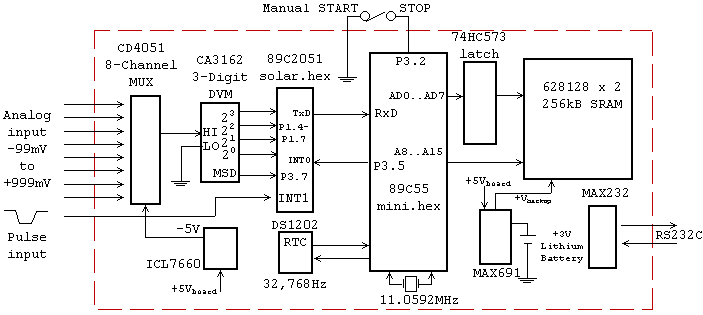
A simplified block diagram of the MiniLOGGER is presented. The CMOS analog multiplexer, 4051, provides output for an 8-channel single-ended input to the analog-to-digital converter chip, CA3162, which operates in free-running mode. The digital output is a 4-bit BCD...
The mine railway connects the national railways and intermediate links of the mining area, serving as an important component of the railway transport network. Statistics indicate that the Chinese mine railway extends over 20,000 kilometers, with numerous road junctions...
Listen and share music wherever you go with the mini speaker system project. This project allows for music playback in various locations such as dorms, cubicles, or the beach. It serves as an excellent introduction to circuit systems, featuring...
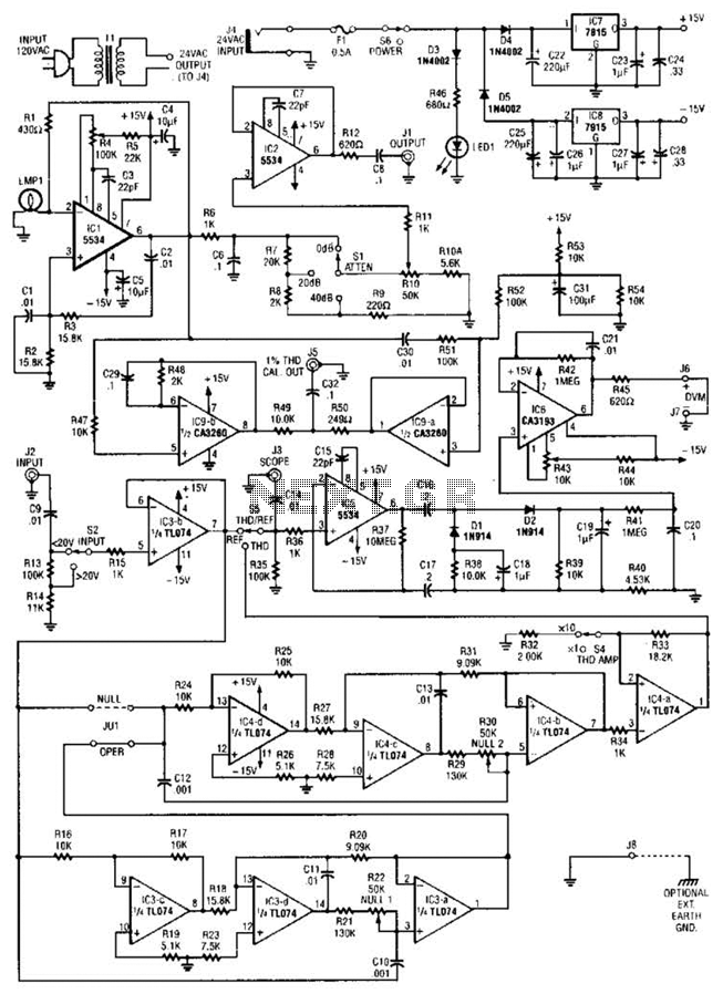
The circuit comprises a low-distortion, 1-kHz oscillator designed to measure Total Harmonic Distortion (THD) at a user-selected voltage level, suitable for voltage amplifiers or for testing amplifiers with power levels up to 600 W. It is capable of detecting...
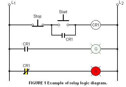
The relay logic circuit creates an electrical schematic diagram for controlling input and output devices. Components include resistors, capacitors, and others. The relay logic circuit operates by utilizing electromechanical relays to control various input and output devices in a systematic...