
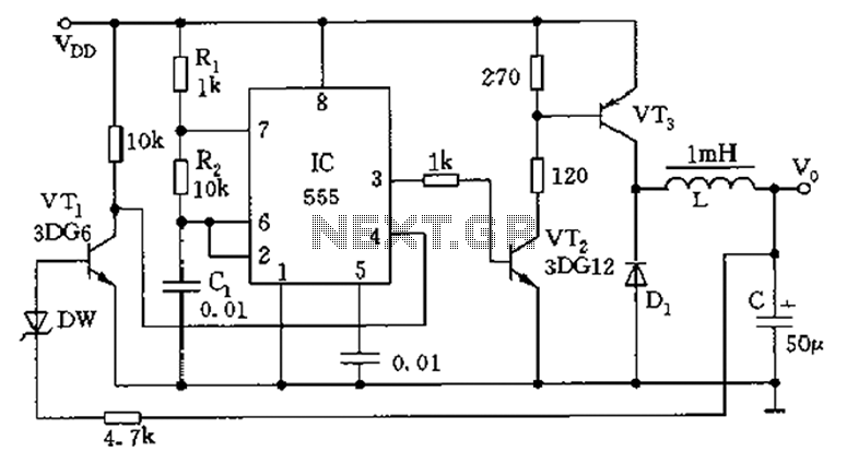
555 monostable trigger timing circuit

The circuit schematic in Figure 3-3 illustrates a monostable configuration of the 555 timer, which is a popular integrated circuit used for timing applications. In this setup, the 555 timer is triggered by a normally open push button switch, which initiates the timing cycle. When the button is pressed, the circuit transitions from a low output state to a high output state, resulting in a voltage increase at the output pin. This transition is facilitated by the internal flip-flop of the 555 timer, which changes state in response to the activation of the push button.
The timing behavior of the circuit is governed by the resistor (R) and capacitor (C) connected to the 555 timer. The time period for which the output remains high, known as the pulse width, is calculated using the formula TW = 1.1RC. This means that the time duration is directly proportional to both the resistance and capacitance values selected. A larger resistor or capacitor will result in a longer output high time, while smaller values will shorten this duration.
When the button is released, the internal discharge switch (Ij1) activates, discharging the capacitor and returning the output to a low state. This allows the circuit to reset and be ready for the next activation. The monostable operation of the 555 timer makes it suitable for applications where a single output pulse is needed in response to an input trigger.
In terms of component selection, the circuit does not impose any stringent requirements, allowing for flexibility in choosing the resistor and capacitor values to achieve the desired timing characteristics. The schematic serves as a fundamental example of how a 555 timer can be employed in a practical circuit for generating timed pulses, showcasing its versatility in electronic design.Introduction to circuit schematic of the circuit shown in Figure 3-3. Here the 555 connected as a one-shot form, usually in a normally open push button switch S-shaped state, pin output low 555. At this point the internal discharge switch Ij1 together, the voltage across capacitor C is zero. When you press the button switch S, the flip-flop flip, 555 feet from low to high, electrical path into the temporary steady state. After Zhe state time, the output end electrostatic level goes low. Transient time - as is the timing TW '- 1. 1RC. This circuit each press switch S, the circuit enters a given working condition once, so this circuit is brother to manually control the development work of the occasion.
(2) Component Component selection parameters as shown in Figure 3-3 shows, wife no special requirements. (3) 555 monostable trigger timing circuit shown in Figure 3-3.
Related Circuits
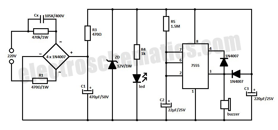
This is a simple power resumption alarm circuit that can be installed within the switch box. It emits beeping sounds when power is restored following a power failure. The power resumption alarm circuit is designed to provide an audible alert...
This device utilizes the MC145026/MC145027 encoding and decoding circuit along with the TDA1808/TDA1809 RF transmitter/receiver module. It can be operated flexibly within a range of 10 to 120 meters, allowing users to maintain the original external appearance and internal...
The program utilizes the internal 4 MHz oscillator of the PIC16F628 microcontroller in a two-input alarm circuit. The two-input alarm circuit designed with the PIC16F628 microcontroller leverages the internal 4 MHz oscillator to provide a stable clock signal for operation....

Using any camera in a dull or dark environment generally requires the use of supplementary light. This is a standard technique, and even where adequate natural light is not available, additional lighting can enhance image quality. In electronic circuit design for...
The circuit consists of a 555 timer configured as an astable multivibrator along with resistors R1 and R2 and capacitor C1. It generates an oscillation frequency of approximately 10 kHz with a duty cycle close to 50%. Transistors VT2...

This is a circuit design for a doorbell that produces a sound resembling that of a bird. The circuit is controlled by an NPN transistor. The operation begins when P1 is set to an experimental value, starting with approximately...