
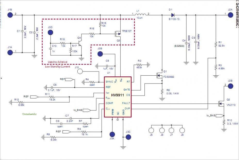
5V Boost Converter using LTC3440

The LTC3440 boost converter is designed to efficiently step up lower input voltages to a stable 5V output, making it suitable for battery-powered applications where maximizing battery life is critical. The device's high efficiency of up to 96% minimizes power loss, allowing for longer operational times between charging cycles. The adjustable oscillator frequency enables the designer to optimize performance based on specific application requirements, such as minimizing electromagnetic interference (EMI) or maximizing efficiency at certain load conditions.
In the circuit configuration, R1 and R2 are critical for setting the output voltage. Their values can be calculated based on the desired output voltage using the feedback network within the LTC3440. The feedback pin monitors the output voltage and adjusts the duty cycle of the internal switching to maintain regulation. R4's value determines the switching frequency of the boost converter, impacting both efficiency and the size of external components.
The frequency compensation network, consisting of R3 and C1, stabilizes the control loop, ensuring that the converter responds appropriately to changes in load and input voltage. C3, as the input bypass capacitor, filters out high-frequency noise and provides a stable input voltage to the IC, while C2, the output filter capacitor, smooths the output voltage, reducing ripple and improving transient response.
The inclusion of S1 allows for easy shutdown of the converter, which can be particularly useful in portable applications where power conservation is essential. Overall, this boost converter circuit, leveraging the capabilities of the LTC3440, provides a reliable and efficient solution for generating a stable 5V output from varying input voltage levels.A simple 5V boost converter using LTC3440 shown here. LTC3440 is a high efficiency DC to DC converter that can be operated from input voltages below, above or equal to the output voltage. As for the synchronous rectification, LTC3440 delivers up to 96% efficiency and up to 600 mA output current is guaranteed.
The IC has built an oscillator whose f requency synchronized whose frequency can be adjusted from 300 kHz to 2 MHz The LTC3440 circuit is connected as a boost converter capable of delivering 5V output 5V @ 300mA constant input voltage of 2. 7 to 4. 2 V. The resistor R4 is used to set the oscillator frequency, while the resistors R1 and R2 are used to adjust the output to 5 volts.
Resistance R3 and capacitor C1 form a frequency compensation network, while C3 serves as an input bypass capacitor. S1 is the stop switch and capacitor C2 is the output filter. 🔗 External reference
Related Circuits
Upon purchasing the slave dial, it arrived without instructions, packaging, or additional details. The only visible markings, aside from decades of grime, were on the face (SMITH SECTRIC, ACELEC SYDNEY) and some markings on the bracket holding the mechanism...
The BQ2000 is a programmable, monolithic integrated circuit designed for fast-charge management of nickel cadmium (NiCd), nickel metal-hydride (NiMH), or lithium-ion (Li-Ion) batteries in single or multi-chemistry applications. The BQ2000 detects the battery chemistry and employs optimal charging and...
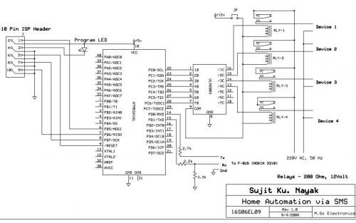
The project involves SMS control for older Nokia phones using the FBUS protocol, which is a complex communication method requiring detailed understanding and coding. The author has successfully implemented this project using an 89S52 microcontroller with only 256 bytes...
A digital thermometer is being planned for construction using an ATmega8 microcontroller and an LM335 temperature sensor. Guidance is sought on how to proceed with the project, particularly concerning the display components. The digital thermometer circuit utilizes the ATmega8 microcontroller,...
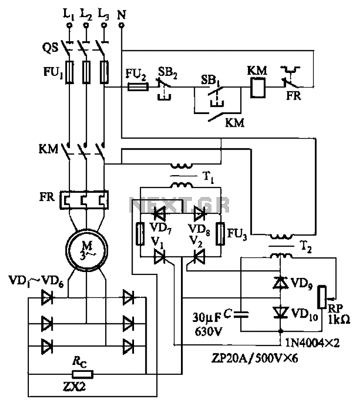
The circuit depicted in Figure 3-171 includes an auxiliary power supply that operates on single-phase AC power. It features a single-phase half-wave controlled bridge composed of diodes VD7, VD8, and thyristors V1, V2. The output current is managed by...
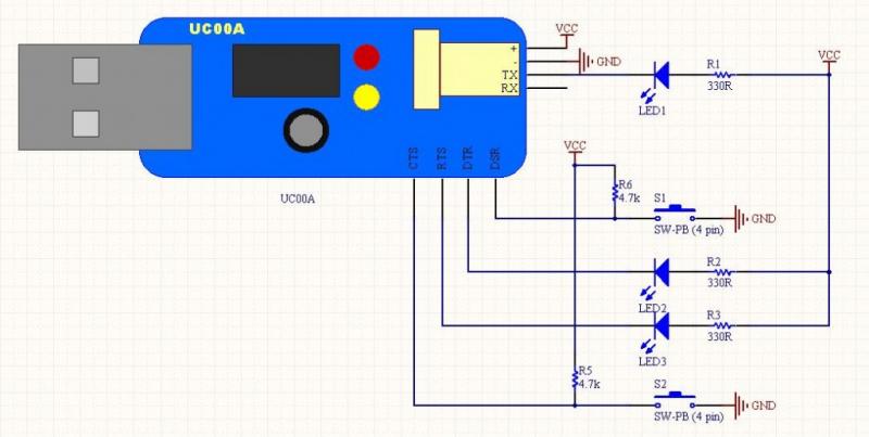
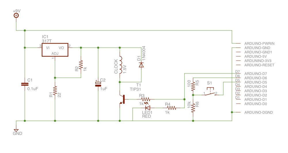
The LEDs operate in an active-low configuration (0), while the initial state of the switches is high (1). In other words, the PC software must send a low signal (0) to activate the LEDs, and if a low signal...