
5W Audio Amplifier Circuit based BD139/BD140

The 5W audio amplifier circuit is designed to deliver efficient audio amplification while maintaining stability and performance across various applications. The choice of BD139 and BD140 transistors allows for robust performance due to their complementary characteristics. The input stage, utilizing a differential amplifier configuration, ensures high input impedance and low output impedance, which is critical for interfacing with audio sources.
The biasing arrangement involving Q1, R3, R4, and the diodes ensures that the transistors operate in the active region, allowing for linear amplification of the audio signal. The current mirror formed by Q4 and Q5 not only provides a stable biasing condition for the differential pair but also enhances the overall gain by maintaining a consistent collector current.
The output stage, driven by Q8, is configured as a common-emitter amplifier, which is known for its high gain and ability to drive loads effectively. The inclusion of Q6 and Q7 as a current mirror helps maintain thermal stability, which is essential for reliable operation, especially in compact designs where heat dissipation may be a concern.
The feedback network plays a crucial role in defining the amplifier's frequency response and overall gain. The values of resistors R5 and R6 can be selected to achieve the desired gain, while capacitors C3 and C4 serve to filter out DC components and provide phase compensation, ensuring the amplifier operates effectively across the audio frequency range.
Overall, this 5W audio amplifier circuit exemplifies a well-balanced design that combines performance, stability, and versatility, making it suitable for a wide range of audio applications.The following is the diagram of 5W audio amplifier circuit which built using power transistor BD139 and BD140 as the final gaining process. This small amplifier can be used as general purpose amplifier such as computer amplifier, radio, mp3 player, video player, etc.
The input stage consists of Q1 through Q5 and 3 diodes. The differential pair is biased by Q1, R3, R4, D3, D4, and D5. The biased current is set to 1 mA. Q4 and Q5 form a current mirror as the active load for the differential pair, and the output is taken out single-endedly from the collector of Q2. The open loop gain of the input stage is more than 60dB. Q8 act as a common-emitter amplifier driving the output stage. Current mirror formed by Q6 and Q7 serve both biasing current source and active load for Q8. The open loop gain of the second stage is about 40dB. Q6 and Q7 are mounted together inside the blue tube to provide thermal compensation to each other. The complimentary pair BD139/140 is biased by D1, D2, and R10. Adjusting the value of R10 can yield the desired quiescent current. R13 and R14 prevent thermal run-away of the complementary pair. DC voltage at the output is always half the power supply. The feedback network consists of R6, R5, C3 and C4. The overall gain is about the ratio of R6 to R5. C4 provides lead compensation; C3 provides DC-blocking. 🔗 External reference
Related Circuits
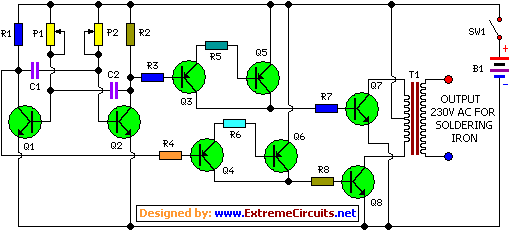
This is a simple and cost-effective inverter designed to power a small soldering iron (25W, 35W, etc.) when a mains supply is not available. The circuit utilizes eight transistors along with several resistors and capacitors. Transistors Q1 and Q2,...
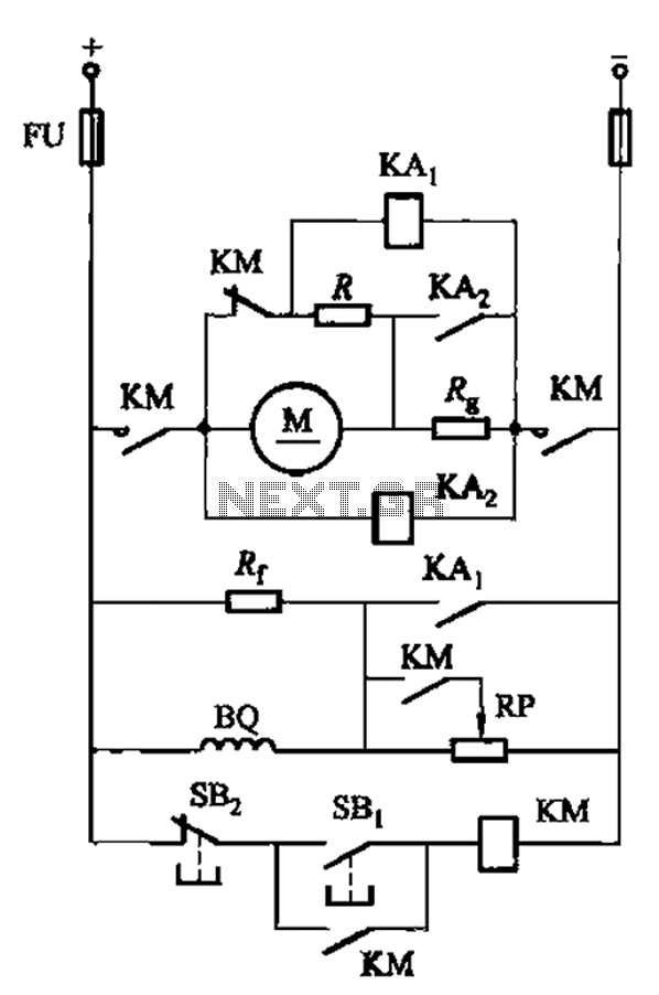
The circuit illustrated in Figure 3-197 features a dish adjust rheostat (RP) that allows for the adjustment of field current, which in turn modifies the motor speed. The circuit operates by utilizing a rheostat, which is a variable resistor that...
Cook in advance to open the door with a coal stove; before using the fire, it should be strong. This is an automatic door opening device that can automatically open the door before the regular homeowner, eliminating the need...
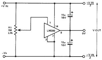
A simple split power supply circuit can be designed using the schematic diagram based on the LM380 audio power integrated circuit (IC). The output voltage regulation is dependent on the circuit feeding the LM380. The power dissipation is approximately...

The circuit diagram illustrates the SF04E emission and the corresponding SF04B. Part (A) depicts the composition of the remote control transmitter SF04E, along with its compatible receiving circuit, which can be assembled using the SJ04H. Part (B) presents the...
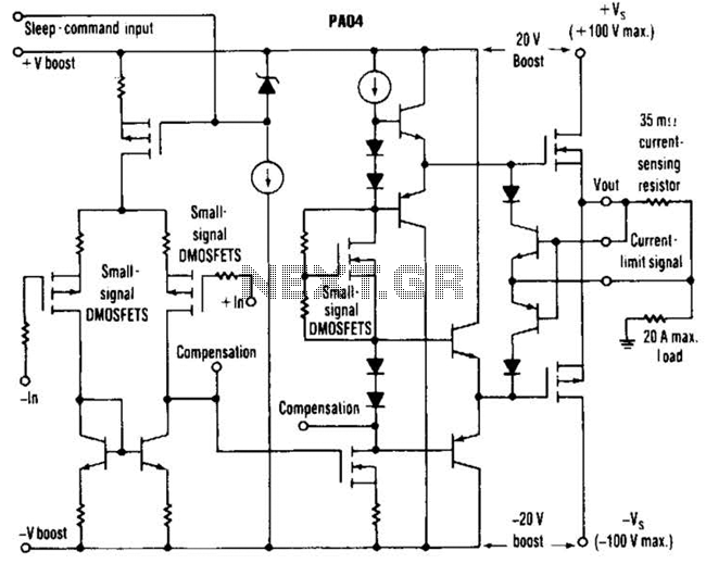
This circuit from Apex Microtechnology can deliver 180 V peak-to-peak at 90 kHz into a 4-ohm load. The PA04 can deliver 400 watts RMS into an 8-ohm load with low total harmonic distortion at frequencies exceeding 20 kHz. The circuit...