
60 LED Clock

The project focuses on utilizing the CD4017 decade counter, which is a popular integrated circuit for counting applications. It counts from 0 to 10 and can be reset to zero, making it suitable for various timing and sequencing applications. The integration of the 4093 NAND gate serves as an oscillator, producing a clock signal necessary for the operation of the 4017. The clock frequency is crucial for determining how quickly the 4017 progresses through its counting sequence.
The choice of resistor and capacitor values for the 4093 is critical; the RC time constant directly influences the frequency of the output clock pulses. The relationship between the resistor (R) and capacitor (C) can be defined by the formula \( f = \frac{1}{2 \pi R C} \), where \( f \) is the frequency. Thus, a 220k ohm resistor and a 4.7µF capacitor yield a frequency of approximately 0.106 Hz, resulting in a one-second pulse.
Proper grounding of unused pins is essential to ensure stable operation. Noise introduced by floating pins can lead to erratic behavior of the circuit, particularly affecting the clock signal. Grounding the specified pins mitigates this issue, providing a more reliable performance of the 4093 NAND gate.
The operation of the circuit is straightforward. The user can switch between the STOP and RUN positions to control the counting process. In the RUN position, the 4017 will count up with each clock pulse generated by the 4093, while in the STOP position, the counting process halts. This simple yet effective design demonstrates the versatility of the 4017 chip in timing applications, providing an excellent platform for further experimentation and learning in electronics.This months project is based on the 4017 chip that we used in a project last month. If you haven`t had a chance to review the basics of the 4017 chip you may want to review the info presented in June`s project of the month. As you can see see we have changed the circuit a little. For example, the 4093 NAND gate is now set to exactly 1 second clock pulses. The clock rate is determined by the resistor and capacitor combination on the 4093. If the resistor is 220k ohms and the capacitor is 4. 7uf then the output will be 1 second clock pulses. To increase the clock rate you should decrease the value of the resistor or capacitor. To decrease the clock rate you should increase the value of the resistor or capacitor. Please remember to ground all unused legs of the 4093 or noise in the circuit will occur and cause the clock to malfunction. Therefore, ground pins 5, 6, 8, 9, 12, and 13. To operate the circuit simply move the switch from STOP to RUN. We aim to transmit more information by carrying articles. Please send us an E-mail to wanghuali@hqew. net within 15 days if we are involved in the problems of article content, copyright or other problems.
We will delete it soon. 🔗 External reference
Related Circuits
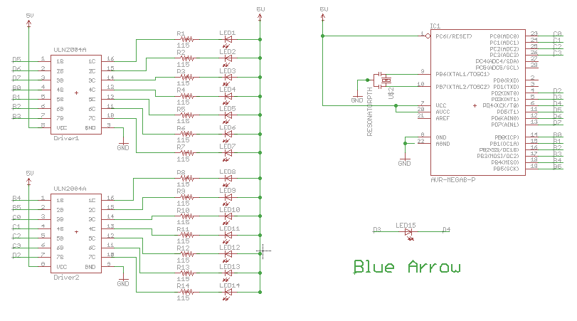
For beginners in microcontroller projects who are unsure where to start, this project serves as one of the simplest options available. It provides a clear understanding of programming a microcontroller. Often, one may glance at a watch and ponder,...
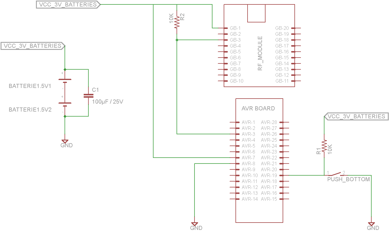
This tutorial demonstrates concepts for creating a lamp with dual actuation. The lamp can be controlled through a parallel switch or by a relay that is managed using an RF module based on the ZigBee protocol (IEEE 802.15.4). The...
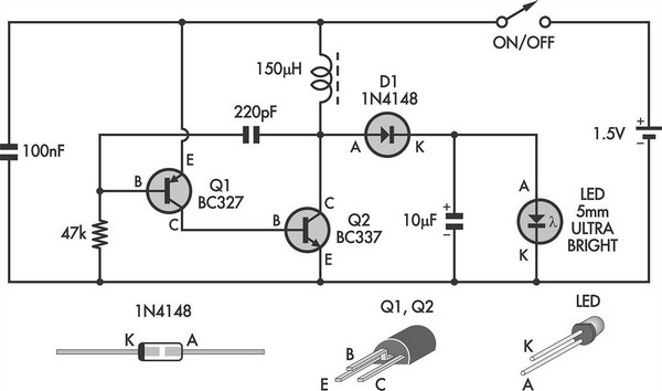
This simple LED torch is driven by a 2-transistor blocking oscillator that steps up the voltage from a 1.5V cell. It relies on the inherent current limiting of the 150 µH choke to protect the white LED from overdrive....
In this project, eight LEDs are connected to PORT B of a PIC microcontroller. A push-button switch is also connected to bit 0 of PORT A using a pull-up resistor. When the switch is pressed, the LEDs scroll to...

Below is a comparator circuit that can measure the voltage of a car battery in steps of 1 volt. The voltage indication is achieved through comparison. The comparator circuit designed for measuring the voltage of a car battery utilizes an...
The design utilizes LEDs as light sensors on a DDR pad, which has been engineered to have no moving parts. Instead of relying on physical feedback, the pad measures light reflectance from the user's feet to detect when an...