
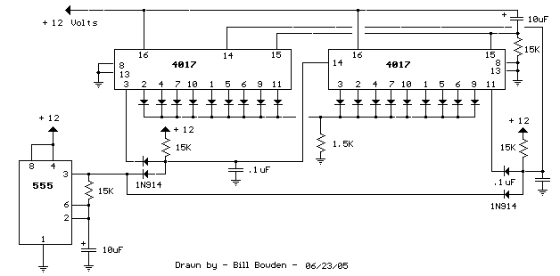
72 LED Clock

The circuit utilizes a combination of 74HCT164 shift registers to create a versatile clock display system. The minute display is achieved through a cascading arrangement of eight shift registers, allowing for a seamless transition between minutes as the single bit circulates through the 60 stages. The interconnections between the registers are crucial, with the cascading nature ensuring that the output of one register feeds into the next. The use of a 47K resistor for feedback from the eighth to the first register is essential for maintaining the continuity of the minute count.
The hour section employs a similar architecture with two 8-bit shift registers, allowing for the display of hours from 1 to 12. The synchronization of the hour and minute registers is facilitated by connecting pin 9 of all registers together, ensuring that the clock operates in unison.
For applications requiring a 50 Hertz operation, the circuit can be modified to accommodate a more complex timing structure, necessitating the additional 74HC30 IC. This allows for the decoding of 7 bits instead of 4, enhancing the precision of the clock's timing function. The grounding of unused NAND gates ensures that the circuit remains stable and free from noise or interference.
The power-on sequence is carefully designed to initialize the registers correctly. The use of a momentary low reset signal coupled with a NAND gate effectively locks out clock transitions during the initialization phase, ensuring that the registers are loaded with the correct initial state. The timing diagram serves as a visual representation of this sequence, detailing the critical moments during the power application and reset process.
User interaction with the clock is facilitated through two push buttons, allowing for easy adjustments of the time settings. The design prioritizes user-friendliness, ensuring that the hours can be set quickly before fine-tuning the minutes. Overall, this circuit design exemplifies a comprehensive approach to creating a functional and user-friendly clock display system using shift registers and LED indicators.In the circuit below, 60 individual LEDs are used to indicate the minutes of a clock and 12 LEDs indicate hours. The power supply and time base circuitry is the same as described in the 28 LED clock circuit above. The minutes section of the clock is comprised of eight 74HCT164 shift registers cascaded so that a single bit can be recirculated through the 60 stages indicating
the appropriate minute of the hour. Only two of the minutes shift registers are shown connected to 16 LEDs. Pin 13 of each register connects to pin 1 of the next for 7 registers. Pin 6 of the 8th register should connect back to pin 1 of the first register using the 47K resistor. Pins 2, 9, 8, 14 and 7 of all 8 minutes registers (74HC164) should be connected in parallel (pin 8 to pin 8, pin 9 to pin 9, etc. ). The hours section contains two 8 bit shift registers and works the same way as the minutes to display 1 of 12 hours.
Pin 9 of all 74HCT164s (hours and minutes) should be connected together. For 50 Hertz operation, the time base section of the circuit can be modified as shown in the lower drawing labeled "50 Hertz LED Clock Time Base". You will need an extra IC (74HC30) to do this since it requires decoding 7 bits of the counter instead of 4.
The two dual input NAND gates (1/2 74HC00) that are not used in the 50 Hertz modification should have their inputs connected to ground. When power is applied, a single "1" bit is loaded into the first stage of both the minutes and hours registers.
To accomplish this, a momentary low reset signal is sent to all the registers (at pin 9) and also a NAND gate to lock out any clock transitions at pin 8 of the minutes registers. At the same time, a high level is applied to the data input lines of both minutes and hours registers at pin 1.
A single positive going clock pulse (at pin 8) is generated at the end of the reset signal which loads a high level into the first stage of the minutes register. The rising edge of first stage output at pin 3 advances the hours (at pin 8) and a single bit is also loaded into the hours register.
Power should remain off for about 3 seconds or more before being re-applied to allow the filter and timing capacitors to discharge. A 1K bleeder resistor is used across the 1000uF filter capacitor to discharge it in about 3 seconds. The timing diagram illustrates the power-on sequence where T1 is the time power is applied and beginning of the reset signal, T2 is the end of the reset signal, T3 is the clock signal to move a high level at pin 1 into the first register, T4 is the end of the data signal.
The time delay from T2 to T3 is exaggerated in the drawing and is actually a very short time of just the propagation delay through the inverter and gate. Two momentary push buttons can be used to set the correct time. The button labeled "M" will increment the minutes slowly and the one labled "H" much faster so that the hours increment slowly.
The hours should be set first, followed by minutes. 🔗 External reference
Related Circuits
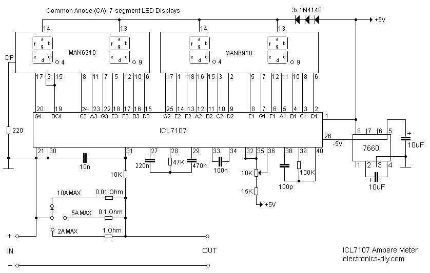
Ammeter is a great addition to any Laboratory Power Supply as it will measure the current consumption and help you determine if there are any problems with the circuit that you are building or testing. This ammeter is capable...
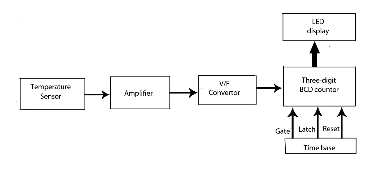
This verified project provides an idea, circuit, and operation of the LED display temperature indicator. It features a digital temperature indicator utilizing a voltage-to-frequency (V/F) converter, along with various electronic projects. The LED display temperature indicator is designed to provide a...
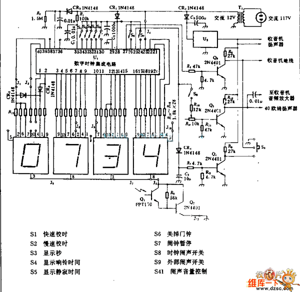
U1 is the 3817 integrated circuit, capable of directly driving the display. It can show time in either 12-hour or 24-hour format, schedule alarm sounds, and automatically turn on the radio at specified times. The display utilizes the FND500...
The question sometimes comes up of how to cascade 4017 decade counters for more than 10 sequential stages. The LED sequencer below shows a possible solution using a few extra parts. When power is applied, the 15K resistor and...
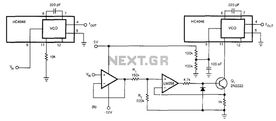
This circuit expands the linear frequency range of an HC4046 from one decade to nearly three decades. An LM358 is utilized as a constant-current sink, replacing the frequency-determining resistor (10 kΩ) connected from pin 9 to ground. For this...
A good way to mount the circuit board is to use a hot glue gun to mold the circuit underneath the lamp housing. There is plenty of space there for your board. At the next photos you can see...