
7W Audio Power Amplifier LF356

The low-frequency output 7W power amplifier circuit is designed for efficient amplification with a focus on stability and protection. The LF356 operational amplifier serves as the core voltage amplification component, leveraging its FET input characteristics to ensure low noise and high input impedance. The use of a negative feedback loop mitigates distortion and enhances linearity, crucial for audio applications.
The coupling circuit formed by C1 and R1 allows for the AC signal to be properly conditioned before reaching the op-amp. The calculated voltage gain of -10 indicates that the output signal will be inverted and amplified tenfold, suitable for driving subsequent stages or loads.
The complementary symmetry arrangement of the output transistors allows for efficient push-pull operation, which is essential in minimizing crossover distortion often found in traditional Class AB amplifiers. The choice of transistors, such as the 2SC1815 and 2SA105, provides a balance between performance and thermal characteristics, ensuring reliable operation under various load conditions.
The overcurrent protection mechanism is a critical feature of this design, preventing potential damage to the output transistors during fault conditions. By monitoring the voltage drop across the emitter resistors, the circuit can effectively limit the output current, thereby protecting the transistors from thermal runaway and ensuring longevity.
Overall, this low-frequency power amplifier circuit exemplifies a robust design approach, integrating feedback, transistor selection, and protective features to deliver reliable performance in audio amplification applications. The inclusion of heat sinks for the output transistors further emphasizes the necessity for thermal management in high-power electronic circuits, ensuring continued operation without failure. As shown for the low-frequency output 7W power amplifier circuit. The circuit uses a FET input type operational amplifier LF356 integrated as a voltage amplification. The class as a transistor amplifier circuit composed of the driver stage. Illustrated circuit has adopted a large negative feedback loop, which feedback resistor R2 is 100k, input terminus C1 (1 F) and R1 (10k ) constituting the coupling circuit. The AC component of the input signal is applied to the op amps inverting input (pin 2), the voltage can be seen, the circuit magnification: Av -R2/R1 -100/10 -10.
Stage amplifier circuit composed of complementary symmetry circuit by the transistor, the transistor connected to form a composite tube, transistor VT1 and VT2 can be 2SC1815, VT5 and VT4 can be used 2SA105, VT3 selection 2SD525, VT6 use 2SB595, after the amp has an overcurrent protection circuit If amplifier tube VT3 (or VT6) output current is too large, then the emitter 0.5 resistor R7 (or R8) will have a greater voltage drop, its polarity is positive on the negative. The voltage applied to VT1 (or VT4) between the base and emitter, so VT1 (or VT4) positively biased conduction (when the external load short-circuit, the saturated conduction), VT1 to VT2 conduction from diversion effect, make VT2 (or VT5) base current decline, thus limiting the VT3 (or VT6) of output current to prevent it from being damaged due to excessive current.
Due to the large VT3 and VT6 power, you need to install the radiator.
Related Circuits
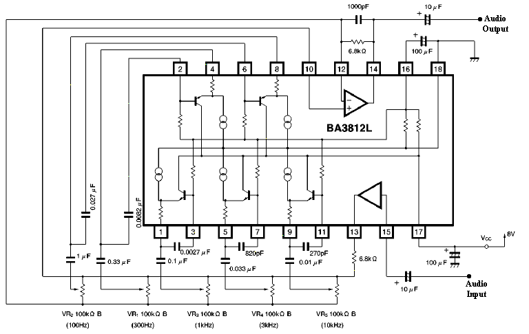
This section discusses a series of 5-band equalizer circuits utilizing a single integrated circuit (IC) BA3812L, which is designed for high-fidelity (hi-fi) audio applications. The BA3812 IC features a 5-point equalizer with all functions integrated within the chip. The...
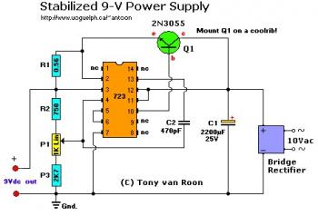
C1 filters the noise and spikes from the AC supply. The circuit can be adjusted to provide a 9V or 12V output voltage, or any other voltage level required by the PC mini drill, using the P1 potentiometer. The circuit...
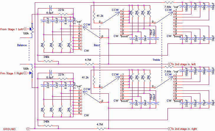
The primary amplifying stages consist of triode-connected 6088 tubes. As previously mentioned, there are two amplifying stages, which provide a non-inverted input to output connection and sufficient gain to include tone control. The tone controls are switch-selected, allowing a...
This circuit illustrates a Car Radio Audio Amplifier using the TDA2003 integrated circuit. The datasheet for the TDA2003 includes electrical characteristics and schematic wiring details. The TDA2003 is a high-performance audio amplifier designed for automotive applications. It is capable of...

This is a simple headphone amplifier. Any NPN transistor can be used. The circuit can be powered by a 9V battery. The headphone amplifier circuit serves to boost audio signals to a level suitable for driving headphones. It typically consists...
The mixer circuit described features three line inputs and three microphone inputs. The microphone inputs are designed for low impedance dynamic microphones with a range of 200 to 1000 ohms. Alternatively, an electret condenser microphone (ECM) can be used,...