
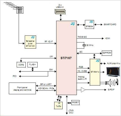
8 Bit Binary to 256 Decimal (1 of 256) Decoder
 Decoder")
The provided description indicates an invitation for contributions to a platform focused on electronics. However, it lacks specific details regarding electronic schematics or circuit designs.
To create a comprehensive electronic schematic description, it is essential to focus on a particular circuit or electronic project. For instance, consider a simple LED blinking circuit using a 555 timer IC.
The circuit consists of a 555 timer configured in astable mode, where it generates a square wave output that alternates the state of the LED. The components required for this circuit include a 555 timer IC, two resistors (R1 and R2), a capacitor (C1), and an LED with a suitable current-limiting resistor (R_LED).
The 555 timer's pins are connected as follows: Pin 1 (GND) to ground, Pin 2 (TRIG) to the junction of R1 and R2, Pin 3 (OUT) to the anode of the LED (through R_LED), Pin 4 (RESET) connected to VCC to disable the reset function, Pin 5 (CTRL) connected to ground via a capacitor for stability, Pin 6 (THRESH) connected to Pin 2, and Pin 7 (DISCH) connected to the junction of R1 and C1. Finally, Pin 8 (VCC) connects to the positive supply voltage.
The timing of the LED blinking is determined by the values of R1, R2, and C1. The duty cycle and frequency of the blinking can be adjusted by changing these component values. This simple yet effective circuit serves as a fundamental example of using a 555 timer in practical applications, illustrating basic principles of timing circuits and LED control.This is a guest post by Olger Groen . If you would like to write for ExtremeCircuits, then drop us an email via contact form or simply comment. A long tim.. 🔗 External reference
Related Circuits
The STK672-050 is a unipolar constant-current chopper-type externally-excited 4-phase stepping motor driver hybrid integrated circuit (IC) that utilizes MOSFET power devices. It features a built-in microstep operation-supported 4-phase distributed controller, enabling the realization of a high torque, low vibration,...
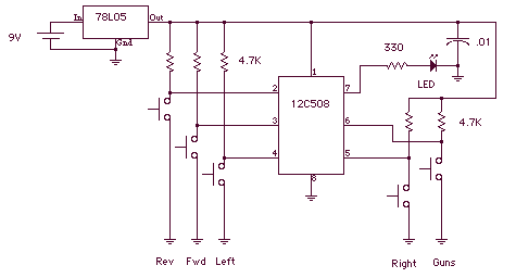
The receiver chip uses a Panasonic 4602 38KHz receiver and that's it for external components. It has the serial input (GP3), two RC hobby servo outputs (GP0/GP1), and three digital outputs (GP2,4,5). Here is the code for the receiver...
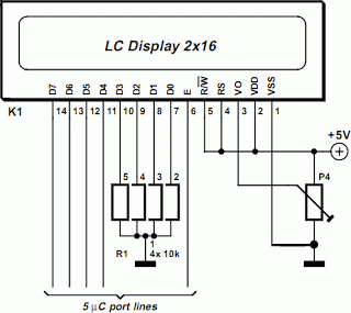
In many projects, alphanumeric LCDs are utilized, which are internally driven by Hitachi's industry-standard HD44780 controller. These displays can be driven... Alphanumeric LCDs that utilize the HD44780 controller are widely used in various electronic projects due to their reliability and...
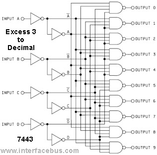
The function diagram for both the 5443 and 5444 integrated circuits (ICs) is identical, assuming a 16-pin dual in-line package. The difference lies in their internal connections, as depicted in the functional schematic, and the method of input decoding....
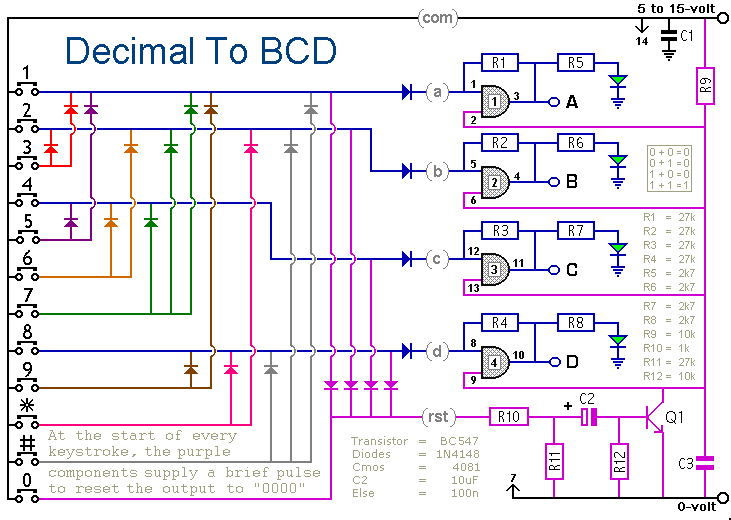
When a keypad switch is pressed, this circuit reproduces its value in Binary Coded Decimal (BCD) format. A 12-keypad is used, but it can be expanded to 16 keys for Hexadecimal to BCD conversion. The circuit consists of two...
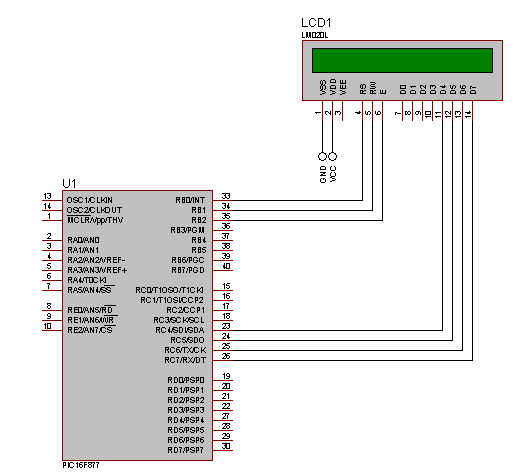
When using an LCD in 4-bit mode, data must be sent twice, whereas in 8-bit mode, it is sent only once. This increases the workload on the microcontroller when interfacing with the LCD. If the microcontroller is handling only...