
A Keypad Circuit That Will Convert From Decimal To BCD Decimal

The circuit design effectively integrates a keypad input with a memory module to provide a stable BCD output. The keypad module, which consists of a matrix of switches, allows users to input numeric values. Each key corresponds to a specific binary value in BCD format. The transient nature of the output from the keypad module is addressed by the memory module, which employs a CMOS 4081 logic gate to latch the output.
Upon pressing a key, the associated logic level is sent to the memory module. The Q1 transistor momentarily pulls the input pins low, ensuring that the previous output state is cleared. This prevents any residual signals from previous keystrokes from affecting the current input. Following this reset, the corresponding signals from the keypad are allowed to latch through resistors R1, R2, R3, and R4, ensuring that the output remains stable until the next key is pressed.
The output pins A, B, C, and D provide the BCD representation of the pressed key. These outputs can be connected to various digital devices or microcontrollers for further processing. The design allows for flexibility in voltage supply, making it suitable for a range of applications. The optional LEDs provide immediate visual feedback on the current BCD output, enhancing usability, although they can be excluded for more compact designs.
Overall, this circuit exemplifies an efficient method for converting keypad inputs into a stable digital format, suitable for integration into larger electronic systems.When a keypad switch is pressed - this circuit will reproduce its value in Binary Coded Decimal from. I`ve used a 12-key pad. But it may be expanded to 16 keys - to provide Hexadecimal to BCD conversion. The circuit is constructed in two parts. There`s a keypad module - and a memory module. On its own - the keypad module only produces a transient output - that disappears the moment you release the switch. But add the memory module - and the output will remain latched - until it`s replaced by the next keystroke. The circuit will work at anything from 5 to 15 vdc. The LEDs are a visual indication of the BCD value. They are not necessary to the operation of the circuit. If you wish - you may leave them out - together with their associated resistors (R5, R6, R7 & R8). The memory module uses a Cmos 4081. At the start of every keystroke - Q1 takes one input pin from each gate low. This resets all four output pins to zero - momentarily. Then any inputs taken high by the keypad - will latch themselves on through R1, R2, R3 & R4. And the new BCD number will be displayed. Note that A, B, C & D are connected directly to the output pins of the Cmos IC. You will need to regulate the load your application places on these outputs. 🔗 External reference
Related Circuits
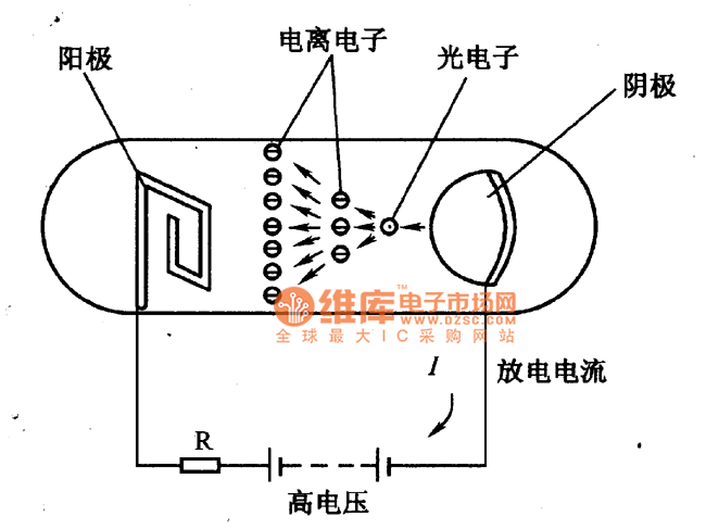
The figure illustrates a schematic circuit of a UV sensor. When voltage is applied between the cathode and anode, and UV radiation passes through the quartz glass tube on the cathode's optical surface, the cathode material, which is coated...
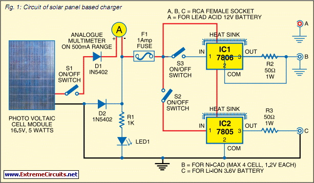
Savings on electricity bills can be achieved by utilizing alternative power sources. The photovoltaic module, or solar panel, described here can provide a power output of 5 watts. Under full sunlight conditions, the solar panel generates an output voltage...
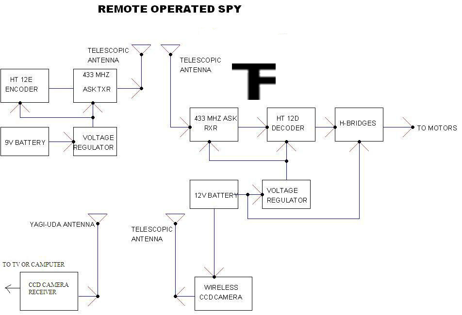
A robot that operates when you send messages through your phone. Your mobile device serves as the remote controller for the robot. This means that if the robot is in London and you are in Mumbai, you can still...
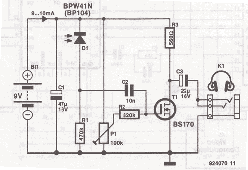
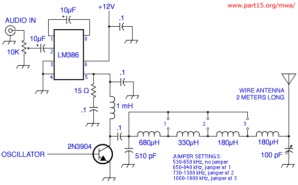
This wireless headphones transmitter ensures quality reception over a distance of 2 meters. The oscillator frequency ranges from 1750 kHz to 3500 kHz, and for the antenna, it... The wireless headphones transmitter operates within a frequency range of 1750 kHz...
If a complete circuit is needed, there are thousands of these circuits available in the designs. Some of them can be provided easily, but further communication is required. The request indicates a need for a comprehensive circuit design, which may...

A BA1404 integrated circuit (IC) is utilized to generate a complete FM multiplex (MPX) signal. The chip incorporates all necessary circuitry. Components CI, R3, R4, and C4 are responsible for providing pre-emphasis. The transmitter operates on a single AA...