
8255 uses 64 input expansion interface circuit

The described computer control system employs the 8255 programmable peripheral interface (PPI) to facilitate the management of multiple digital signal inputs. The 8255 chip is a versatile device that provides three 8-bit parallel I/O ports, thereby enabling the connection of up to 24 digital signals per chip. This capability is essential for applications requiring extensive input handling, such as automated control systems or data acquisition setups.
To implement the system, the 8255 chips need to be properly initialized through a microcontroller or microprocessor, which configures the chip's operational mode and sets the necessary control registers. This initialization process is crucial as it determines how the I/O ports will function—whether as input or output, and the mode of operation (e.g., mode 0 for simple I/O, mode 1 for strobed I/O, or mode 2 for bidirectional data transfer).
For a system that requires handling 64 input signals, as depicted in Figure 27-29, a total of three 8255 chips would be necessary, as each chip can handle 24 signals, allowing for a total of 72 signals. The design should incorporate adequate power supply considerations, as well as signal conditioning components, to ensure reliable operation of the inputs. Additionally, the circuit should include pull-up resistors on the input lines to prevent floating states and ensure stable readings.
The schematic should clearly depict the connections between the microcontroller, the 8255 chips, and the input signal sources. It is also advisable to include decoupling capacitors near the power pins of the 8255 chips to minimize noise and ensure stable operation. Overall, the circuit design must account for the physical layout, ensuring proper grounding and minimizing interference from adjacent components.Computer control system, you can detect the signal path switching means dressing a lot, you need a lot of input interface expansion Wei, so can all switch signal input into the computer. When using a programmable chip 8255 expansion input interface, there are 8255 per piece 3 1/0, pass through the program in its entirety is initialized to enter work, you can enter up to 24 digital signals, therefore, according to the switching signal input large ones it can calculate the required number of 8255 chips. Figure 27-29 shows using 8255 expansion interface circuit 64 inputs.
Related Circuits

The circuit depicted in Figure 3-135 employs a time relay (KT) to determine the braking time. The circuit utilizes a time relay, which is a crucial component for controlling the duration of the braking process. The time relay KT is...
Without a USB to phone battery charger circuit, charging a phone battery using a USB port on a computer can quickly damage the battery, resulting in bulging. This occurs because the voltage output from USB is 5 volts, while...
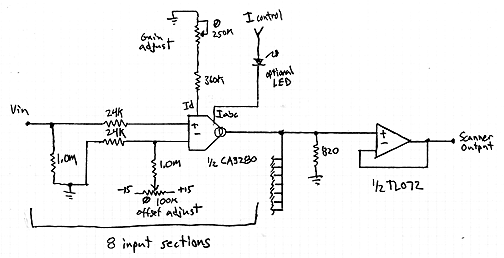
This design is for an interpolating scanner, a circuit featuring multiple signal inputs, a control voltage input, and a signal output. The output selectively transitions between inputs, smoothly fading from one to the next as the control voltage increases....
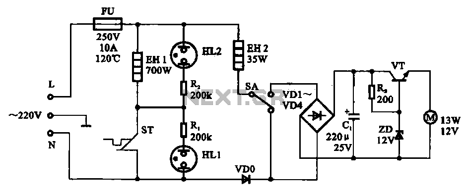
The electric thermos temperature detection control circuit is designed to monitor and manage the temperature within an electric thermos. It primarily consists of a control circuit for the boiler heater and heater insulation, an electrical magnetic pump motor drive...
A voltage supply ranging from 6 V to 15 V is required when using a single LED per module. An increase in the number of LEDs necessitates a corresponding increase in the voltage supply, with additional LEDs connected in...
The LM4910 typical circuit is designed for a two-channel amplifier. The left and right channel audio signals are input to the LM4910 (in an MSOP/SO package) at pins 1 and 2. The output signals are delivered from pins 6,...