
A DC-RRS Application Circuit

The DC solid-state relay (DC-SSR) serves as a crucial component in controlling high-power loads, providing a reliable means of switching without mechanical contacts. The schematic typically includes a control input, which activates the relay, and an output that connects to the load. In the context of high-power applications, the DC-SSR is designed to handle substantial current and voltage levels, making it suitable for various industrial and commercial applications.
The input side of the DC-SSR is typically connected to a low-voltage control signal, which can be sourced from a microcontroller or a control circuit. Upon receiving the control signal, the internal opto-isolator activates the semiconductor switching element, usually a transistor or a triac, allowing current to flow through the output circuit.
The output circuit is connected to the high-power load, which can include motors, heaters, or other heavy-duty electrical devices. It is essential to ensure that the DC-SSR is rated for the specific load current and voltage to prevent overheating and potential failure. Additionally, heat dissipation mechanisms, such as heat sinks or fans, may be incorporated to maintain optimal operating temperatures.
Protection components, such as fuses or circuit breakers, are often included in the circuit design to safeguard against overload conditions. Snubber circuits may also be employed to suppress voltage spikes generated during switching events, thus protecting the relay and the load.
In summary, the integration of a DC solid-state relay in a high-power load circuit provides efficient control and reliability, essential for modern electronic applications requiring robust performance and safety.DC solid state relay (DC-SSR) driving high-power load circuit is shown in (a) below; high power load driving circuit shown in (b) below.
Related Circuits

If you need a timer circuit, we go after the most proven 555. However, if the delays are longer, based on timing capacitor capacity is too large. In this case, a circuit of Figure 1 After pressing the button...
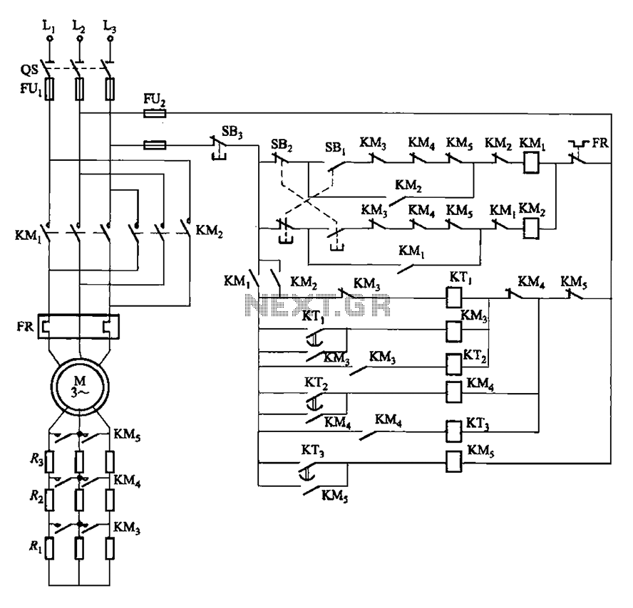
The circuit depicted in Figure 3-162 includes several components: SBi serves as the forward start button, SBz functions as the reverse start button, and SB3 is designated as the stop button. The resistance levels for the start switches are...

The following circuit illustrates a Repeating Interval Timer Circuit Diagram. This circuit is based on the CMOS 4060 integrated circuit (IC). Features include a 6-pin output. The Repeating Interval Timer Circuit utilizing the CMOS 4060 IC is designed to generate...
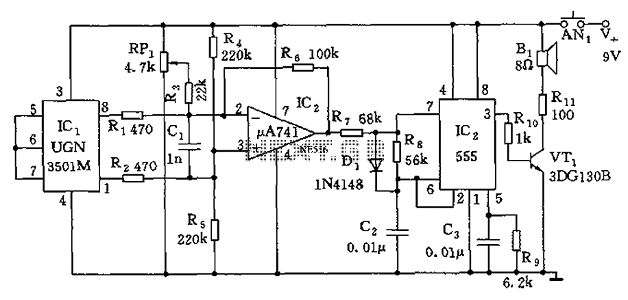
The circuit consists of a 555 timer and associated components designed for voltage-to-frequency conversion. It is utilized for determining the orientation of Earth's magnetic field using a Hall-effect sensor, specifically the UGN-3501M. This sensor incorporates a Hall element and...
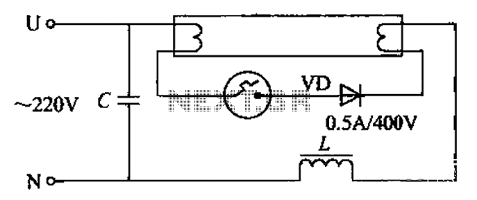
By incorporating a second pull tube into the circuit during the starter ionization phase, the positive half-cycle diode conduction results in an approximate DC current flow. This current is rectified, and due to the small ballast impedance, the instantaneous...
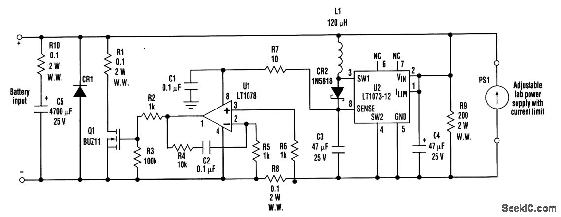
When developing a battery charger, using a real battery can be impractical. The battery simulator circuit described here serves as an alternative. The positive and negative terminals of the battery input should be connected in place of the actual...