
A new stable RC pulse generator

This circuit design illustrates a versatile multivibrator configuration that can be adapted for various applications requiring precise timing and duty cycle control. The use of separate timing resistors allows for tailored output characteristics, making it suitable for a wide range of electronic applications, including pulse-width modulation, timing circuits, and signal generation. The careful selection of diodes and resistor values ensures optimal performance, even under varying temperature and power supply conditions. The ability to maintain stability and PSRR while adjusting pulse width and frequency independently is a significant advantage, enhancing the usability of this circuit in practical scenarios.This familiar circuit can be implemented with any rail-to-rail-output comparator or the venerable LMC555. The output period is given by 2log(2)RC = 1. 386RC, and the stability is better than ±100 ppm/ °C against temperature and ±100 ppm/V against power-supply variation.
But if an output duty cycle different than 50:50 is needed, application of this simple circuit gets complicated. That`s because the usual ways in which the basic RC multivibrator is modified for asymmetrical output timing either allow annoying interaction between output duty cycle and period or degrade the tempco and the PSRR. But a new twist to this old circuit ( Fig. 2 ) adds a few diodes to the traditional recipe to allow independent adjustment of pulse width and period while retaining the good frequency stability of the standard topology.
The new modification starts with an old idea ”addition of diodes D1 and D2 so that the positive and negative phases of the output cycle are controlled by separate timing resistors R1 and R2. This trick works well and is a handy way to implement a multivibrator with an arbitrary output on/off ratio.
The trouble is that D1 and D2`s temperature-dependent diode voltage drops (Vds) can drastically erode both the multivibrator`s output period temperature coefficient and PSRR. Canceling these effects, accomplished with compensation diodes D3 and D4, is the gimmick featured in Figure 2.
If Vd3 = Vd1 and Vd4 = Vd2, Figure 3 reveals how the duration of the positive output pulse is now given by: Static Vd effects thus cancel and leave the output period unchanged from the original Figure 1 circuit, which has no diodes at all. Admittedly, this approximation ignores the fact that due to variation in charging current over the RC timing cycle, the various Vds aren`t perfectly constant.
Even so, canceling diode effects good enough so that matched diode tempcos add no more than about + ppm/ °C to the oscillator period temperature dependence. The excellent PSRR of the original circuit is similarly preserved. The new topology makes various novel timing circuits possible, one which is illustrated in Figure 4. Here, pulse width and frequency are independently adjusted by R1 and R3, respectively. The reason pulse frequency is independent of R1 is that total pulse period is given by: But (R1 + R2) = RPOT, which is constant and independent of position the potentiometer wiper.
Meanwhile, the pot wiper position determines and, therefore, pulse width (PW 0. 693R1C) independent of R3. For most combinations of R and values, D1 through D4 can be simple switching diodes, such as the 1N4148. But for higher R values, where junction leakage can become a significant factor, better performance will be obtained if transistor collector-base diodes (e.
g. , 2N3904) are used. 🔗 External reference
Related Circuits
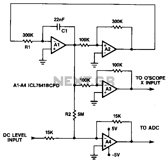
This circuit generates a symmetrical 10 mV peak-to-peak triangle waveform that is summed with a DC level and connected to the analog input for noise and DNL testing. The DC level input offsets the triangle waveform over the input...
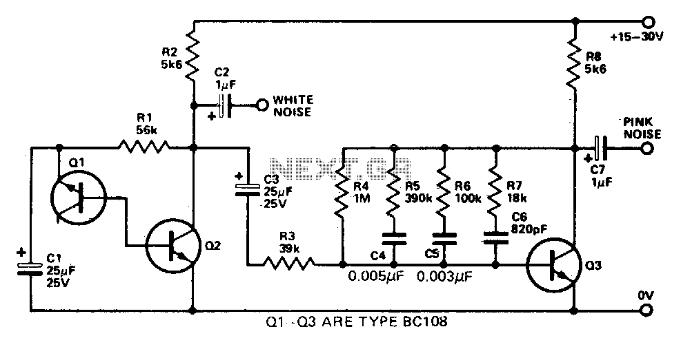
This simple circuit generates both white and pink noise. Transistor Q1 functions as a zener diode, with the base-emitter junction being reverse-biased to achieve zener breakdown at approximately 7 to 8 volts. The zener noise current from Q1 flows...

This circuit generates speed pulses from the speed-dependent voltage spikes produced by commonly used types of PC power supply fans, which are superimposed. The circuit utilizes the voltage spikes generated by the fan's operation to create a series of speed...

Adjustable Regulated Power Supply 0-15V 1A. The output voltage is stabilized and regulated in the range of 0V to 15V, with a maximum current supply of 1A. The schematic diagram originates from the circuit: Adjustable Regulated Power Supply 0-15V...
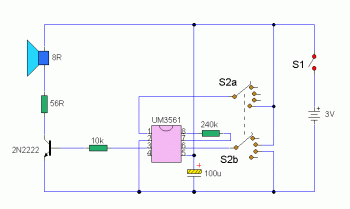
This schematic is simple and easy to construct. The integrated circuit (IC) generates all the sound effects, with the output at Pin 3 being amplified by a transistor. A 64-ohm loudspeaker can be used instead of the 56-ohm resistor...
A 555 timer and a dual 556 timer are used to generate a basic video signal, as illustrated in the schematic. The first timer operates in astable mode, producing synchronization pulses with a period ranging from 4.7 to 8...