
A simple control circuit Lantern

The schematic described involves a primary voltage reduction from the 220V mains supply, which is essential for safe operation in low-voltage electronic devices. The control circuit utilizes a series of components to manage voltage levels and ensure stable operation. The inclusion of a voltage regulator allows for a consistent +9V output, which is crucial for powering sensitive electronic components.
The control port (G) acts as the interface for external signals, allowing for adjustments to the circuit's behavior based on user input or environmental changes. The transistor (TG1) is responsible for amplifying the control signals to drive the vibration mechanism, which can be used in various applications, including audio devices and other electronic systems that require dynamic feedback.
Resistors (R) are strategically placed within the circuit to limit current and protect sensitive components from overload. The design also features capacitors (C) that serve as filters to smooth out voltage fluctuations, ensuring a stable output. The diodes (D2, D3) are critical for indicating the operational status of the oscillator, allowing for easy troubleshooting and maintenance.
The variable frequency oscillator is a key element in this design, enabling the adjustment of output frequencies to match specific requirements. This feature is particularly beneficial in audio applications, where frequency modulation can enhance sound quality and performance. Overall, this circuit design exemplifies a robust approach to managing high-voltage inputs while providing a reliable low-voltage output for various electronic applications.220V mains drop by n guanidine D. Yi stream. C. After the spike Bode + 9V voltage supply control circuit. Port G, TG1 to Shang tube vibration: R. w, and hurricane.. w Partial e agle as base resistance: R4, hurricane to pull the load collector il; C, f. Weeding table for the capacitor; D2 D3 is made Wherever: rice tube, Sichuan to indicate oscillator work like two exhausted withered rough 1. w/Ir Pei variable frequency vibration caries: Day, W, C4, c, Hungary hoof audio input. Kl disobedient cry for the conversion. Dial in vain r Fu wash when color. sparkle frequency i rate a .J 0 Head section chief, dial-sectional 2 - color -) TI-l sparkle * ji Jazz Music Festival with impaired rhythm coup s coup.
Related Circuits
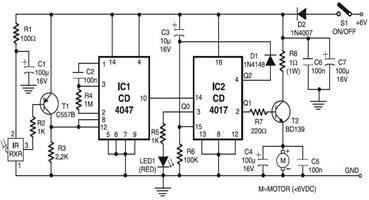
The following circuit illustrates an infrared toy car motor controller. This circuit is based on the 4047 and 4017 integrated circuits (ICs). Features: 16V. The infrared toy car motor controller circuit utilizes two primary integrated circuits, the 4047 and the...
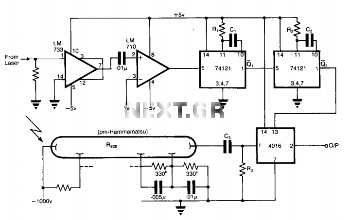
The application involves observing the light pulse emerging from a thick specimen after transillumination by a laser pulse. Pulses derived from the laser source are amplified using a Video Amplifier LM733. The reference level is set to 1 V...
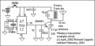
This section describes an experimental low power, low bandwidth data signaling system that was initially made to operate at 55 MHz (television channel 2 in the U.S.). Before operating a radio transmitter, find out what kind of transmitter operation,...
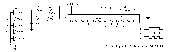
Generating long delays of several hours can be achieved using a low-frequency oscillator and a binary counter. A single Schmitt Trigger inverter stage (1/6 of 74HC14) functions as a square wave oscillator, producing a low frequency of approximately 0.5...
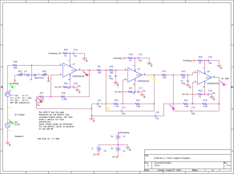
A bandwidth-limited amplifier shapes the waveform sampled by the 40 MHz high-speed pipeline Analog to Digital Converter (fast ADC, or fADC). It is well known that the shaping time is twice the time constant (peaking time) for each pole...
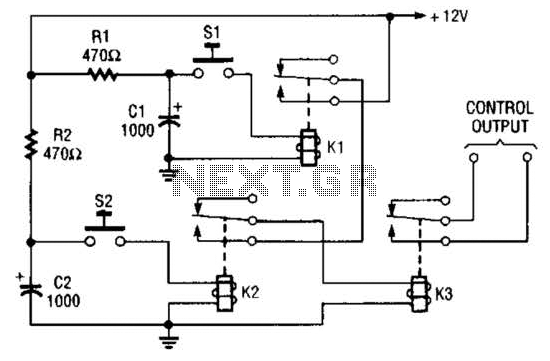
Due to the limited hold-on time of the delay circuits R1/C1 and R2/C2, both switches S1 and S2 must be activated simultaneously to energize the load. The circuit in question involves a delay mechanism governed by the time constants associated...