
Active Antenna I

The circuit employs a two-transistor configuration to achieve impedance matching between the short pull-up antenna and the receiver. The first transistor, Q1, is configured as a common emitter amplifier, which provides high input impedance essential for effectively coupling the high output impedance of the antenna. This configuration minimizes signal loss and maximizes the transfer of the radio frequency (RF) signal from the antenna to the circuit.
Transistor Q2, configured as a common collector (emitter follower), presents a low output impedance to the receiver. This arrangement ensures that the output signal from Q2 is suitable for the low input impedance of the receiver, allowing for efficient signal transfer. The combination of Q1 and Q2 creates a broadband amplifier that operates effectively across the specified frequency range of 100 kHz to 30 MHz, making it suitable for various RF applications.
The circuit design also incorporates biasing resistors to stabilize the operating points of the transistors, ensuring consistent performance across varying environmental conditions. Capacitive coupling may be employed at the input and output stages to block any DC components from the antenna or receiver, allowing only the AC RF signals to pass through.
In summary, this circuit design effectively transforms the characteristics of a short pull-up antenna, enabling it to perform similarly to a long wire antenna while maintaining a high level of signal integrity across a broad frequency range, without introducing voltage gain. The careful selection and arrangement of components within the impedance-matching network are critical to achieving optimal performance in RF signal reception. This circuit is designed to make a short pull-up antenna perform like a long wire antenna, while offering no voltage gain. The circuit boosts the receiver"s performance only if the signal at the antenna is of sufficient level to begin with. This circuit takes a short pull-up antenna that has a high output impedance and couples it to the receiver"s low input impedance through a two-transistor impedance-matching network.
Transistor Ql"s high input impedance and high-frequency characteristics make it a good match for the short antenna, and Q2"s low output impedance is a close match for the receiver"s input. This circuit is usable over the range from 100 kHz to 30 MHz.
Related Circuits
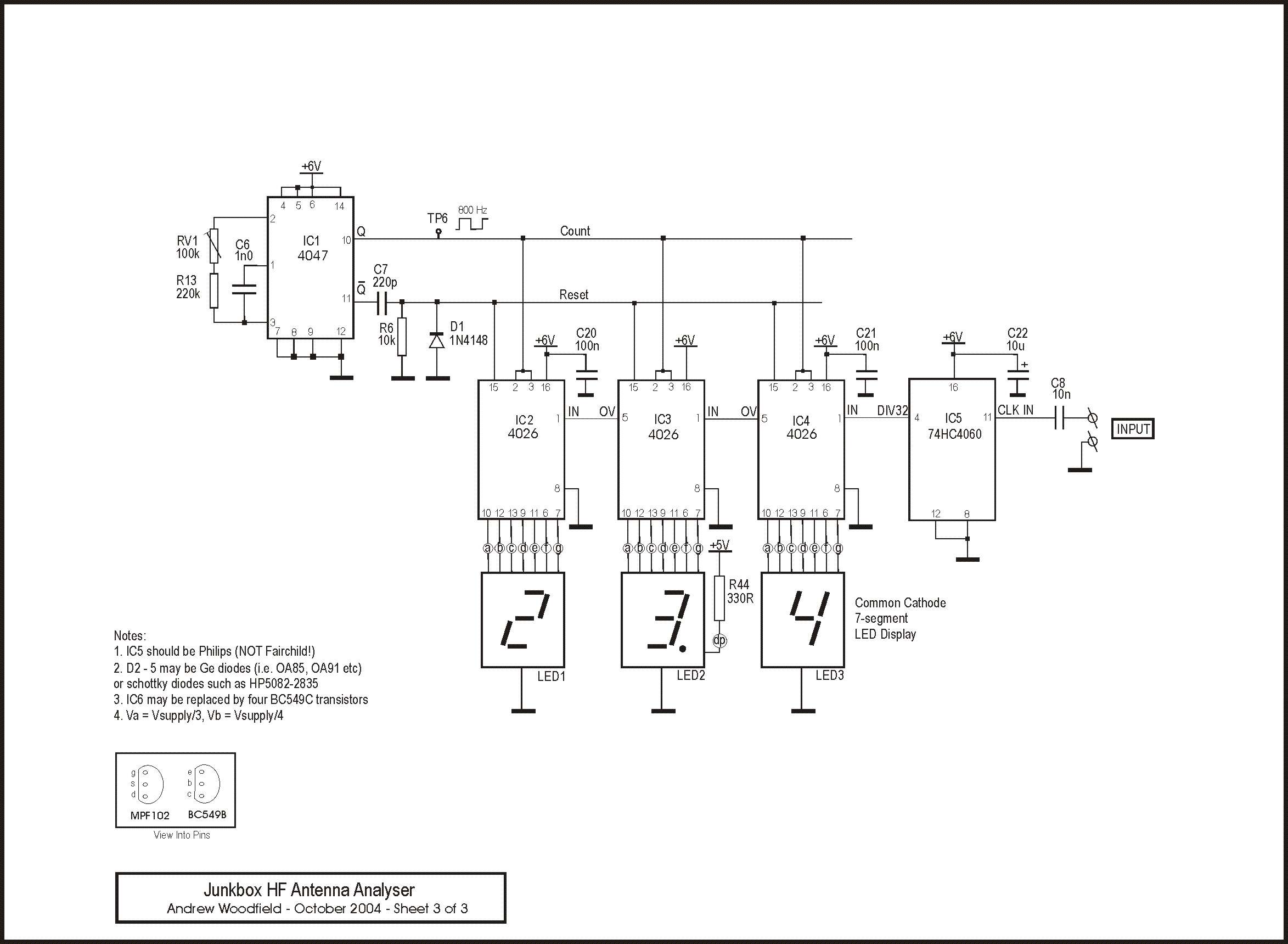
Results are displayed on an analog VSWR meter. The design was originally published in Break-In, New Zealand's amateur radio magazine in September/October 2005, and is republished here with the editor's permission. Note: Break-In is a term used in amateur...
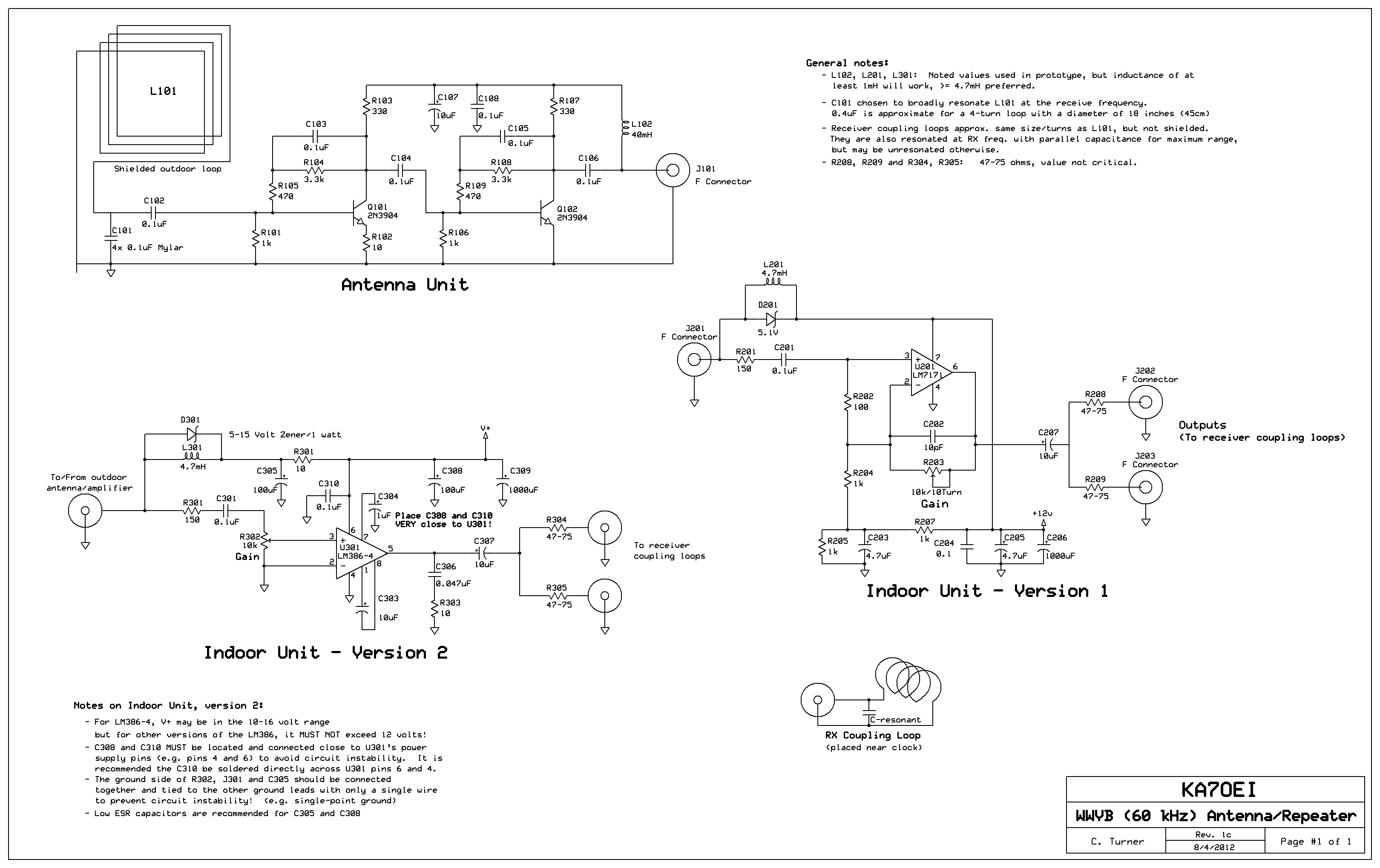
Inside the outdoor box where the loop is mounted, the amplifier circuitry is displayed. The four capacitors located at the lower-left corner of the perfboard are used to broadly resonate the receive loop. In the office building, which is...
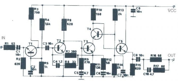
The T1 transistor must be of the BF200 type (or a similar variant), while the other transistors can be of the BF214 type. To achieve high efficiency, the antenna amplifier should be positioned at a short distance from the...
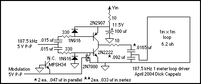
This 1 square meter antenna has radiation resistance of about 10 nanohoms, making the 0.4 Ohm resistance (including skin effect, which about doubled the resistance from the DC value) the dominant loss in the antenna. The lower the resistance,...
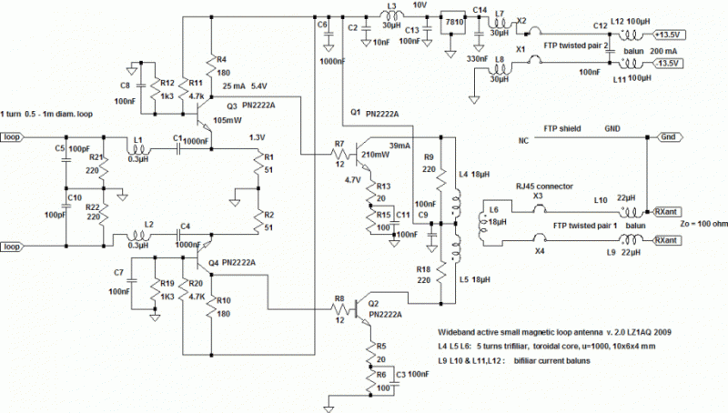
There are extremely wideband software-defined radios (SDR) where a wideband antenna is a natural choice. Wideband small magnetic loops (WSM loops) have been used for 3-4 decades, and their effectiveness as a wideband SDR input is under evaluation. The...

The CYWUSB6953 is a comprehensive Radio System-on-Chip (SoC) device that facilitates the implementation of various simple RF systems using a single chip and a few discrete components. It is specifically designed for low-cost wireless systems that operate within the...