
Loop antenna for 187 KHz

More: In the U.S., the Federal Communications Commission rules limit unlicensed transmitters in the 160 to 190 kHz band to a maximum input power to 1 watt and maximum antenna length of 15 meters. With such a small antenna compared to wavelength, the radiation resistance would be very low, and real (Ohmic) resistance in the antenna would tend to be a lot larger than the radiation resistance, making the antenna even less efficient. This puts a premium on getting the real resistance of the antenna as low as one practically can. Some have made antennae from copper water pipe and RG 8/U coax shield, and they would be more efficient for their size than this one, which used 0.5 square mm copper wire. This output stage has a rich lineage. Murray Greeman, ZLBPU is credited as the originator of the circuit as an LF output stage. Bill Ashlock found that the output signal was cleaner when the transistors had separate base driver resistors. I chose to move the clamping diodes to the end of the base resistors connected to the transistor bases and eliminate the third resistor in the base circuit that was in common with both inputs.
I encourage you to do an internet search on Murray Greeman ZLBPU, Bill Ashlock, and Lyle Kehler for more information on Lowfer transmitter and antennas. Here are some URL's to get you started. Though these links worked on the day I created this page, I don't make any promises to keep them up-to-date.
I added a 2N7000 to gate the NPN output transistor as a means to modulate the stage with either CW (A1) or tone bursts (quasi-A2). I damaged several 2N7000's with ESD in earlier experiments and have started adding gate protection to some circuits. Here, an MPSH34 (chosen for no other reason than because I have a lot of them) is used. Signals below ground are clamped to one diode drop below ground. Signals more positive than about +6 volts are clamped by avalanching emitter-base junction. On the breadboard, the avalanche voltage was measured at 5.8 volts when the emitter was biased with 1.8 milliamps.
The described antenna operates at low frequencies, specifically within the 160 to 190 kHz band, where efficiency is critical due to the inherent limitations imposed by its small physical size relative to the wavelength. The antenna's construction utilizes 0.5 mm² copper wire arranged in a square loop configuration, measuring one meter on each side. The low radiation resistance of approximately 10 nanohoms presents significant challenges, as the dominant resistance is primarily due to Ohmic losses, which are exacerbated by skin effect.
The efficiency of the antenna is inversely proportional to its resistance; thus, efforts to minimize resistance are paramount. The design choices, including the use of copper wire instead of alternative materials like copper water pipes or coaxial shield, directly impact the overall performance. The output stage of the circuit is influenced by historical designs, notably those attributed to Murray Greeman and further refined by Bill Ashlock.
The circuit employs a 2N7000 transistor for modulation purposes, facilitating Continuous Wave (CW) or tone burst signals. To protect against electrostatic discharge (ESD), additional gate protection measures are included, utilizing an MPSH34 transistor. The design incorporates clamping diodes to manage signal levels effectively, ensuring that voltages remain within safe operational limits. The measured avalanche voltage of 5.8 volts is indicative of careful biasing and component selection, contributing to the overall integrity of the circuit.
This arrangement not only enhances the efficiency of the antenna but also ensures reliable operation in the designated frequency range, adhering to regulatory requirements while optimizing performance characteristics. This 1 square meter antenna has radiation resistance of about 10 nanohoms, making the 0.4 Ohm resistance (including skin effect, which about doubled the resistance from the DC value) the dominant loss in the antenna. The lower the resistance, the more efficient it would be - and from these numbers, efficiency is nearly directly proportional to 1/R; cut the resistance in half and double the efficiency.
The antenna, which is a square loop of 0.5 square mm copper wire 1 meter on each side, measured 6.2 uH and under 0.2 ohms DC. In the U.S., the Federal Communications Commission rules limit unlicensed transmitters in the 160 to 190 kHz band to a maximum input power to 1 watt and maximum antenna length of 15 meters. With such a small antenna compared to wavelength, the radiation resistance would be very low, and real (Ohmic) resistance in the antenna would tend to be a lot larger than the radiation resistance, making the antenna even less efficient.
This puts a premium on getting the real resistance of the antenna as low as one practically can. Some have made antennae from copper water pipe and RG 8/U coax shield, and they would be more efficient for their size than this one, which used 0.5 square mm copper wire. This output stage has a rich lineage. Murray Greeman, ZLBPU is credited as the originator of the circuit as an LF output stage. Bill Ashlock found that the output signal was cleaner when the transistors has separate base driver resistors.
I chose to move the clamping diodes to the end of the base resistors connected to the transistor bases and eliminate the third resistor in the base circuit that was in common with both inputs. I encourage you to do an internet search on Murray Greeman ZLBPU, Bill Ashlock, and Lyle Kehler) for more information on Lowfer transmitter and antennas.
Here are some URL's to get you started. Though these links worked on the day I created this page, I don't make any promises to keep them up-to-date. I added a 2N7000 to gate the NPN output transistor as a means to modulate the stage with either CW (A1) or tone bursts (quasi-A2).
I damaged several 2N7000's with ESD in earlier experiments and have started adding gate protection to some circuits. Here, an MPSH34 (chosen for no other reason than because I have a lot of them) is used. Signals below ground are clamped to one diode drop below ground. Signals more positive than about +6 volts are clamped by avalanching emitter-base junction. On the breadboard, the avalanche voltage was measured at 5.8 volts when the emitter was biased with 1.8 milliamps.
🔗 External reference
Related Circuits
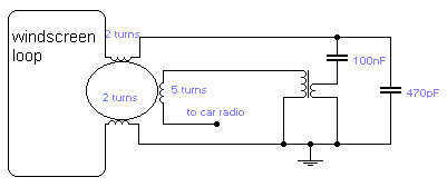
If you do not like the whip antenna on your car, you may try this alternative circuit. A one-turn loop is installed in the windscreen of the car, keeping possibly away from the metal structure of the car. This...

This simple filter utilizes an RC section as the filter element, incorporating a voltage follower to manage other frequencies. The -3 dB point is calculated as 1/(6.28 * RXCV), resulting in a response that drops 6 dB per octave...
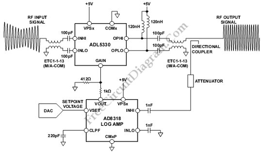
This is a circuit for Closed-Loop Automatic Power Control for RF Applications. The circuit utilizes a log detector (AD8318) and a variable gain amplifier (VGA) (ADL5330). The Closed-Loop Automatic Power Control (APC) circuit is designed to maintain a consistent output...
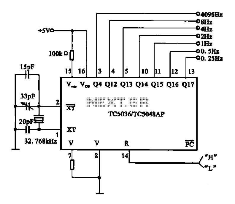
32.768 kHz; In MP3/MP4 devices, mobile phones, laptops, and other digital products, a real-time clock signal generating circuit is utilized, primarily composed of crystal resonators and TC5036/TC5048AP chip oscillators. This setup produces a raw 32.768 kHz crystal oscillator signal,...
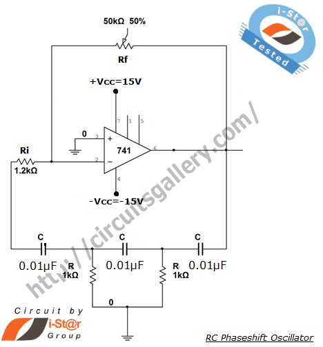
A phase-shifted oscillator can be constructed using a basic operational amplifier (op-amp), three resistors, and three capacitors. One of the resistors should be adjustable, while the other components should have the same value. This oscillator design exhibits low distortion...

This UHF antenna amplifier circuit, also referred to as a UHF antenna booster circuit, is designed to amplify signals within the UHF band, specifically from 400 MHz to 850 MHz. The circuit employs a single transistor and provides an...