
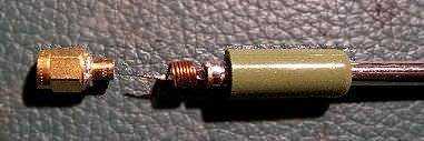
Active FM Antenna Booster circuit

The circuit features two inductors, L1 and L2, which are critical components in the FM antenna booster design. L1, with four turns, is designed to provide a certain inductance value that enhances the input signal. The use of 20 SWG enamelled copper wire ensures good conductivity and minimizes losses due to resistance. The slightly spaced winding technique may be employed to reduce the coupling between the turns, which can help in tuning the circuit's resonant frequency.
Coil L2, having three turns, serves a similar function but may be tailored for a different frequency or gain requirement. The difference in the number of turns between L1 and L2 allows for fine-tuning of the circuit's performance characteristics. The tapping of L1 at the first turn from the ground lead side indicates that this point may be used for feedback or signal extraction, which is essential for maintaining stability and enhancing the overall gain of the amplifier.
The transistor 2SC2570 is a key active component in this circuit, and its pin configuration is crucial for proper integration into the schematic. This transistor is typically used in RF applications due to its favorable frequency response and gain characteristics. The configuration must be adhered to ensure that the transistor operates within its optimal range.
Adjustable trimmers VC1 and VC2 are included in the design to allow for precise tuning of the input and output stages of the amplifier. By manipulating these trimmers, the user can achieve maximum gain, which is vital for effective signal amplification in an FM antenna application. Proper adjustment ensures that the circuit operates efficiently, minimizing distortion and maximizing signal clarity.
Overall, this schematic emphasizes the importance of component selection and configuration in achieving optimal performance in an FM antenna booster circuit.Input coil L1 consists of four turns of 20SWG enamelled copper wire (slightly space wound) over 5mm diameter former. It is tapped at the first turn from ground lead side. Coil L2 is similar to L1, but has only three turns. Pin configuration of transistor 2SC2570 is shown in the fm antenna booster schematic. Adjust input/output trimmers (VC1/VC2) for maximum gain. 🔗 External reference
Related Circuits
You can make your own 2-meter "rubber duckies" that will likely perform much better than many commercial units. I compared my design with two other "rubber duckies" of the TH215 and ICT7 which outperformed them both. With the "duckie"...

This circuit is used to select modes of operation. The accelerometer is utilized to generally move the snake arm, while the Hall effect sensors are designed to enable various functions. The circuit described incorporates an accelerometer and Hall effect sensors...
The MP4 audio circuitry consists of audio D/A converters and an audio amplifier combination circuit. This design features a straightforward circuit layout, making it suitable for integration into compact MP4 digital devices. The MP4 audio circuitry is designed to efficiently...
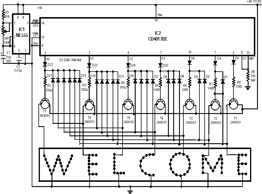
Running Message Display Circuit Diagram. This circuit is based on the CD401 IC. Features: Light emitting diodes are advantageous due to their smaller size. The Running Message Display Circuit utilizes the CD401 integrated circuit, which is a versatile component in...
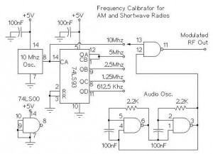
The following circuit illustrates an AM/Shortwave Radio Frequency Calibrator Circuit Diagram. This circuit is based on the 74LS93 IC. Features: The .. The AM/Shortwave Radio Frequency Calibrator Circuit utilizes the 74LS93 integrated circuit, which is a 4-bit binary counter. This...
The sections available in this datasheet cover general design considerations for the 555 timer, frequently asked application questions (FAQ), design formulas, and examples of innovative applications. Examples of applications include a Missing Pulse Detector, Pulse Width Modulation (PWM), Tone...