
AD574 and PC bus interface circuit

The circuit described involves the integration of an AD574 analog-to-digital converter (ADC) with a PC bus architecture, facilitating the conversion of analog signals into digital form for processing. The AD574 is a precision ADC that operates with a resolution of 12 bits, allowing for accurate representation of analog inputs.
In this configuration, U1 (AD574) receives the analog signal and converts it into a digital output. U2 (74LS245) serves as a bidirectional data buffer, enabling the digital data from the ADC to be transmitted to the PC bus while also allowing data to flow back from the bus to the ADC if necessary. This feature is crucial for maintaining signal integrity and for managing bidirectional communication effectively.
U3 (74LS00) is a dual two-input AND gate that can be utilized for various logical operations within the circuit. This component can be employed to control the flow of data based on certain conditions, ensuring that the digital signals are processed only when specific criteria are met.
U4 (74LS125) is a quad tri-state buffer, which allows the output to be either driven high, driven low, or placed in a high-impedance state. This functionality is essential for bus systems, as it prevents contention on the bus when multiple devices are connected, allowing only one device to drive the bus at any given time.
U5 (74LS04) is a hex inverter that inverts the input signals. This gate can be used to manipulate the logic levels within the circuit, providing flexibility in signal processing and control.
Overall, this circuit exemplifies a typical application of digital logic components in conjunction with an ADC to create a robust interface between analog and digital systems, suitable for use in various electronic applications requiring data acquisition and processing.Another example given in AD574 and PC bus. The figure for the AD574 converter Ul, U2 is 74LS245 bidirectional data buffer, U3 of 74 Lsoo two-input AND gate, U4 to 74LS125 tri-s tate output gates, U5 is 74LS04 inverting gate.
Related Circuits
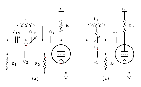
The circuit operates in a parallel-fed configuration, as the DC plate current does not pass through the inductor. R3 can be substituted with an RF choke if desired. Capacitor C3 prevents B+ from appearing across the variable capacitor, which...
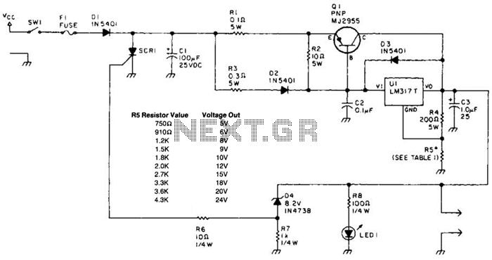
A laptop computer power supply that provides a 9-V output, includes crowbar overvoltage protection, and operates from a 12-V input supply is described. The input supply voltage must be at least 3.6 V above the desired output voltage. The...
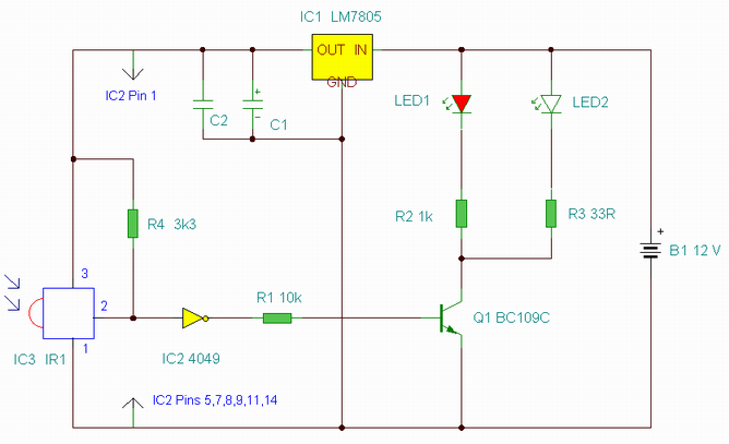
This is an enhanced infrared (IR) remote control extender circuit. It features high noise immunity, resistance to ambient and reflected light, and an increased operational range. The improved IR remote control extender circuit is designed to extend the range of...
This infrared alarm barrier is designed to detect individuals passing through doorways, corridors, and small gates. The transmitter emits an invisible beam of infrared light. When this beam is interrupted by a person, a buzzer connected to the receiver...
Writing about multiple circuits in Marx, an entire new set has been discovered, referred to as "the" Marx Generator. There are diagrams available, along with a useful quote: "The main advantage of the Marx circuit configuration over a more...
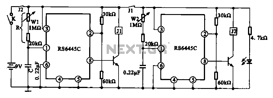
The timing integrated circuit (IC) RS6445C functions as a blocking oscillator. It features two segments, WI and W2, which are utilized to adjust the working time and the closure time. These adjustments can be continuously set within a range...