
Adder circuit

The inverting adder circuit operates based on the principle of superposition. Each input voltage is applied through its respective resistor to the inverting terminal of the operational amplifier. The output voltage (V_out) can be expressed mathematically as V_out = - (R_f/R_i) * (V_1 + V_2 + V_3 + ... + V_n), where R_f is the feedback resistor and R_i represents the input resistors corresponding to each input voltage. The negative sign indicates that the output is inverted relative to the input signals.
In the typical configuration, the operational amplifier's inverting input is connected to the junction of the input resistors. The feedback resistor R_f connects from the output back to the inverting input, creating a feedback loop essential for the operation of the amplifier. The non-inverting input is typically grounded or connected to a reference voltage, ensuring stability in the circuit.
The balancing resistor R4 plays a critical role in maintaining the correct gain and stability of the circuit. Its value is chosen to match the equivalent resistance of the input resistors to minimize offset errors and ensure accurate summation of the input signals. The design allows for flexible scaling of the output voltage by adjusting the feedback and input resistors, thus enabling the circuit to accommodate a variety of applications, such as audio mixing, signal processing, and data acquisition systems.
Overall, the inverting adder circuit is a fundamental building block in analog electronics, providing a straightforward method for summing multiple voltage signals while maintaining control over the gain and phase characteristics.Adder circuit commonly used inverting input, namely the inverting adder circuit. It was to the inverting input of the operational amplifier electrical path, based on the signal voltage to be added through a resistor connected to the inverting input terminal of the operational amplifier. Adder circuit shown in Figure 7-5, which is having a three input inverting adder circuit. Wherein the input signal number eight ii, machine 2,1113 are N input from the inverting input terminal, pin feedback resistors, non-inverting input terminal P via the balancing resistor R4 connected to.
The resistance value of the balancing resistor R4 vase should be Ri, R2, R3 and the parallel and Rr. The output voltage of adder circuit input voltage is equal to the sum of the branch, which kind of structure can be realized adder plurality of input signals.
Related Circuits
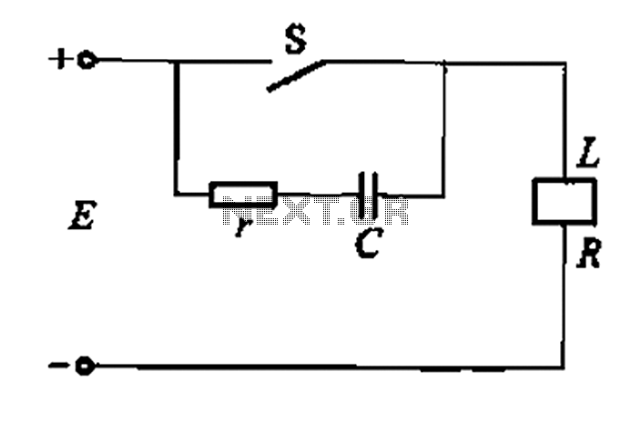
A resistor-capacitor circuit designed to prevent spark blowout. The coil's magnetic energy is converted into electrical energy stored in the capacitance C, effectively suppressing sparks and enhancing safety. The circuit is capable of functioning normally even with reverse polarity....
This design circuit project involves a clear glass sensor circuit intended for experimental or hobbyist applications. The concept is straightforward and relies on a homemade sensor unit that includes one high-efficiency ultra-bright red LED (D1) and a standard phototransistor. The...
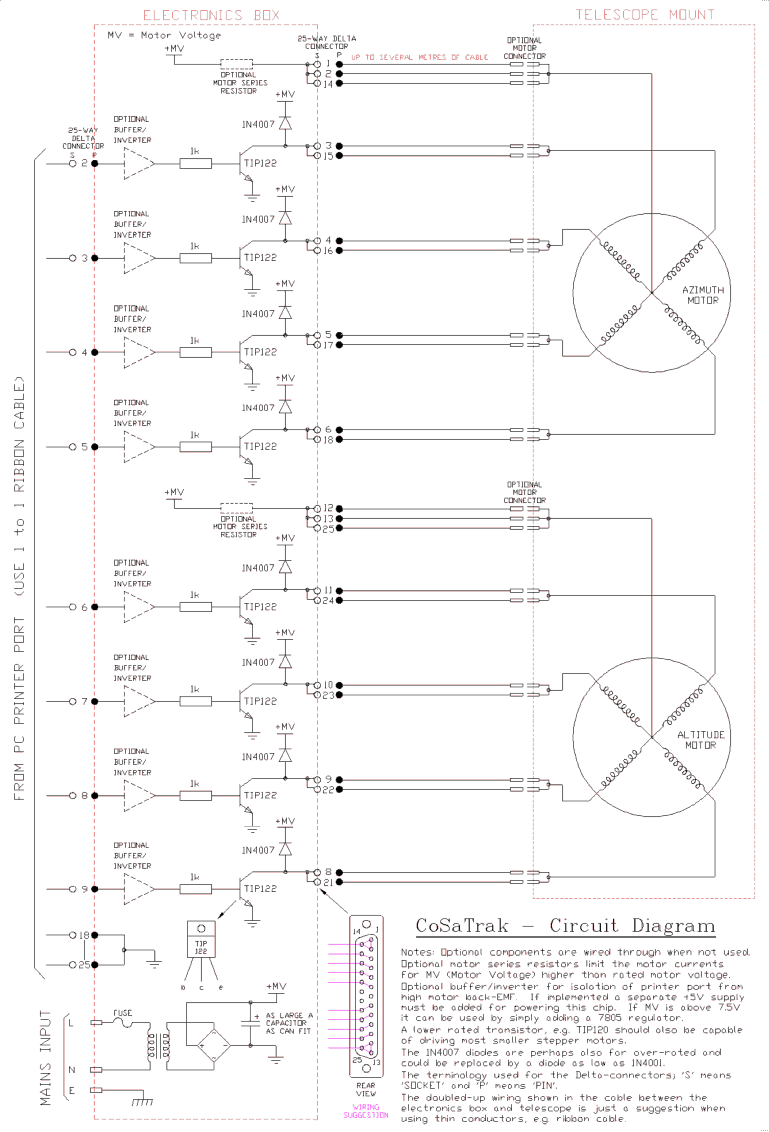
The back EMF voltage spikes produced by stepper motors, especially higher voltage motors, can damage a PC's printer port if connections are made incorrectly, flyback diodes are absent, or connected in reverse. The safest options are opto-isolated or buffered/inverted...
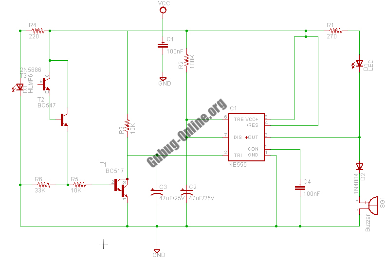
The circuit is based on the NE555 timer, functioning as a simple noise maker, with its output connected to a single transistor oscillator. This oscillator is designed to operate within a frequency range of 800 MHz to 2 GHz,...
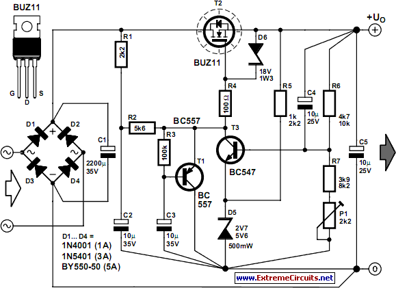
The circuit diagram illustrates a voltage regulator designed from discrete components to meet specific voltage requirements. It provides two sets of component values for output voltages of 6.3 V (upper) and 12.6 V (lower). The components used include BC547...
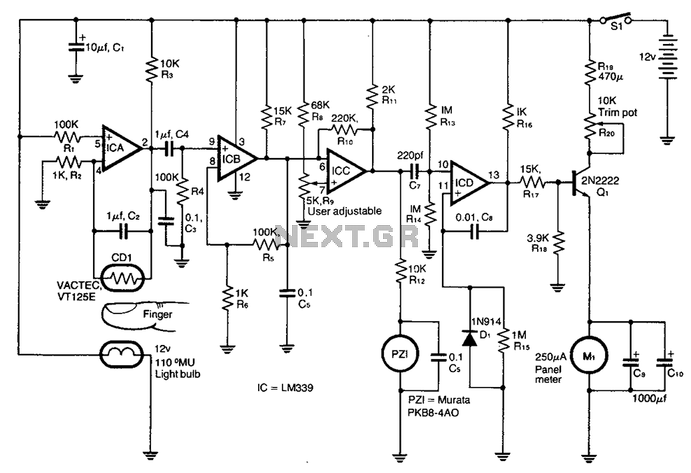
A cadmium sulfide photoresistor (CD1) fingertip can be detected through the filter. CD1 forms part of the sense amplifier feedback network. A section of the sense amplifier (ICA) produces weak signals that may be further amplified by ICB. These...