
Agc System For Audio Signals Circuit

The AGC circuit operates by maintaining a consistent output level despite variations in the input signal amplitude. The operational amplifier is configured to amplify the input signal, while the rectifier section converts the amplified AC signal into a DC voltage that is proportional to the signal's amplitude. This DC voltage is then used to control the impedance of the transistor Q1 and diode D1, effectively adjusting the gain of the amplifier based on the input level.
The use of the voltage divider in the input stage allows for precise control over the input signal level before it reaches the op-amp, ensuring that the signal remains within the optimal range for amplification. The configuration of Rs, RL, and CB in the rectifier section is critical for achieving the desired response time and frequency characteristics of the AGC system. Capacitor C2 plays a vital role in stabilizing the circuit by removing any DC offset that could interfere with the operation of the AGC.
Overall, this AGC circuit design is advantageous for audio applications where maintaining a uniform output level is essential, such as in radio transmitters, audio processing equipment, and communication systems. The integration of the amplifier and rectifier into a single op-amp simplifies the design and enhances reliability while maintaining cost-effectiveness. This circuit is an AGC system for audio-frequency signals. AGC systems usually consist of three parts: an amplifier, rectifier, and controlled impedance. In this circuit the functions of an amplifier and a rectifier are performed by a single op amp. This makes the system simple and cheap.The rectifier is made with the output push-pull cascade of the op amp and Rs, RL, and CB. The transistor Ql and D1 are used as a voltage-controlled resistance (Z). The input signal is (Z + R^/Z times, diminished by the voltage divider and 1 + R2/Ri times, amplified by the op amp. C2 eliminates influence of dc bias voltage. R3 protects Ql and D1 from excessive current.
Related Circuits
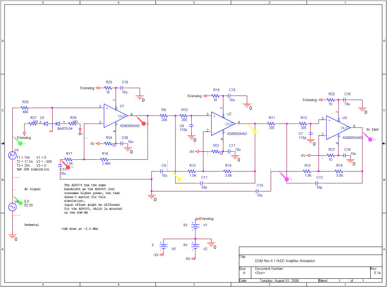
A bandwidth-limited amplifier shapes the waveform sampled by the 40 MHz high-speed pipeline Analog to Digital Converter (fast ADC, or fADC). It is well known that the shaping time is twice the time constant (peaking time) for each pole...
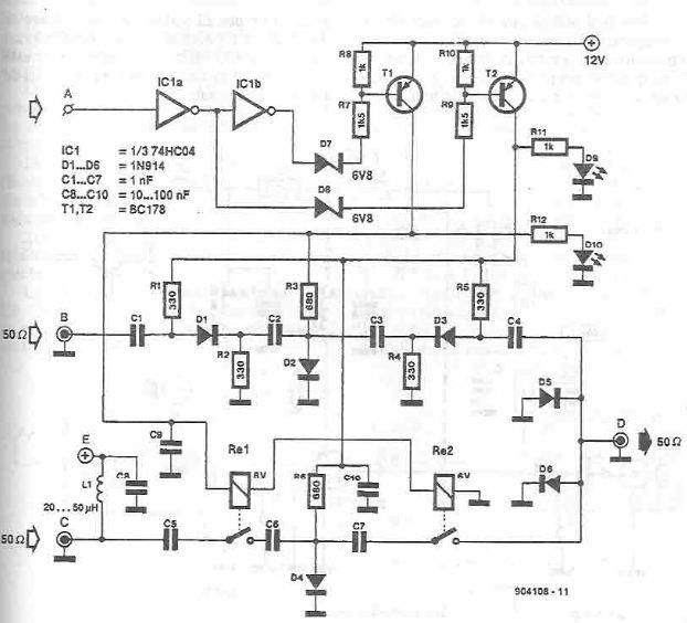
This antenna selector circuit diagram electronic project is constructed using standard electronic components and facilitates the switching between two FM antennas through a logic signal. The gates IC1b and IC1a manage the switching and interface between the required logic...
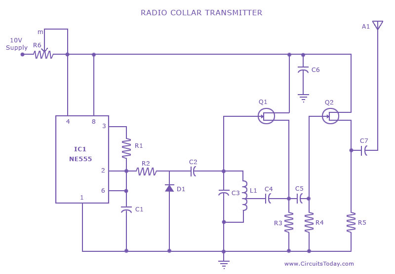
This is a radio transmitter circuit diagram designed for integration into radio collars using the NE 555 integrated circuit. The circuit transmits a pulse in the FM band, specifically between 88 MHz and 105 MHz. The radio transmitter circuit utilizes...

Many Joule Thief circuits traditionally rely on a bulky toroidal inductor that requires careful winding with copper wire. However, there are now compact 4-legged integrated circuits (ICs) available that can perform the same function using only a simple inductor,...
The circuit demonstrates the application of the ZN414 integrated circuit (IC) to create a compact AM radio receiver. The ZN414 IC is a combination of a transistor and a tuned radio frequency (TRF) circuit. The ZN414 IC is specifically designed...
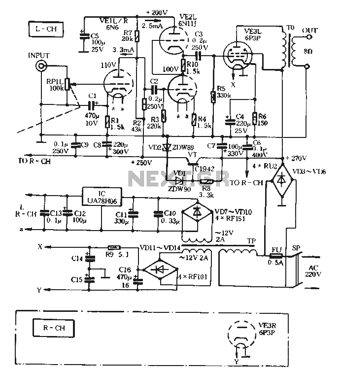
The VE1 preamplifier utilizes a low muscle, low resistance double triode 6N6 configuration, with separate halves for the left and right audio channels. The design operates within the CPI framework. It promotes the use of high-level VE2 household low...