
am rf amp for internal antenna circuit

The circuit utilizes a standard NPN transistor, with the 2N3904 being a common choice, although the 2N2222A is also suitable. The selection of a low noise transistor is recommended to enhance performance, particularly in radio applications. The radio in question typically connects to a ferrite bar antenna with three primary connections: the antenna connection to the tuning capacitor, a ground connection formed by twisting two wires together, and a secondary connection that represents a smaller number of turns on the antenna winding.
In this configuration, the twisted wires serve as the ground reference, while the secondary wire is wired to the base of the transistor. This arrangement allows the transistor to receive its base bias directly from the radio's circuitry. The resistor R1 is crucial for setting the appropriate biasing conditions based on the supply voltage of the radio. The recommended resistor values are as follows: 56kΩ for a 9V supply, 47kΩ for a 6V supply, and 33kΩ for a 3V supply. This biasing ensures that the collector of the transistor operates around half of the supply voltage, optimizing the transistor's performance in the circuit.
The schematic presented is designed for a negative ground configuration. In scenarios involving a positive ground radio, it is essential to replace the NPN transistor with a PNP transistor to maintain proper functionality and signal integrity. This design consideration is critical for ensuring that the circuit operates effectively within the intended application.Any NPN transistor can be used. The author used a 2N3904, but a 2N2222A should work just as well. A good, low noise transistor would be even better. Some radios only have three connections to their ferrite bar antenna: the antenna connection to the tuning capacitor, ground (two wires twisted together) and secondary (the smaller number of turns). I n this case, treat the twisted wires as ground, and the secondary wire as the base connection to the transistor. The transistor will then receive its base bias from the radio. R1 changes with the supply voltage. If your radio is 9V, use 56K. If it is 6V, use 47k. If it is 3V, use 33k. The goal is to bias the collector of the transistor to one half the supply voltage. The schematic shown is for a negative ground radio. For a positive ground radio, substitute a PNP transistor. 🔗 External reference
Related Circuits
Stepping motor controllers are frequently preferred over complex software-driven controllers due to their low cost. However, stepping motors tend to exhibit low torque at high speeds, necessitating a starting ramp to avoid stalling during startup. This circuit provides a...
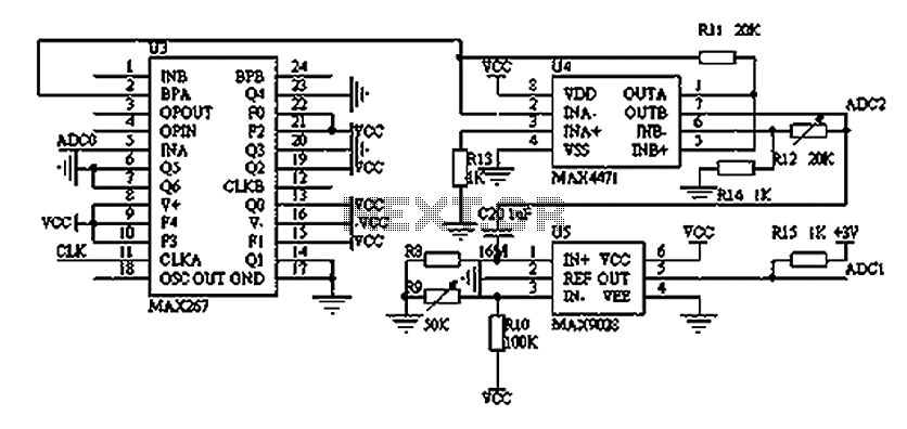
The filtering and amplifying circuit consists of two main components. The MAXIM MAX267 filter is an integrated circuit that can function as a low-pass, band-pass, high-pass filter, and other configurations, offering superior performance compared to traditional op-amp filters. The...

Surround Sound Decoder circuit diagram. The circuit's operation begins when the stereo sound signal carries surround sound information through the master volume section. This drives the Left channel (Lch), which is connected to Model TL072 IC1A and IC1B, with...
This infrared alarm barrier is designed to detect individuals passing through doorways, corridors, and small gates. The transmitter emits an invisible beam of infrared light. When this beam is interrupted by a person, a buzzer connected to the receiver...

This is the circuit diagram of a UHF band TV antenna booster with a 15dB gain power. This low-cost antenna booster is simple and easy to build. This circuit is based on the BF180 UHF transistor. The first stage...
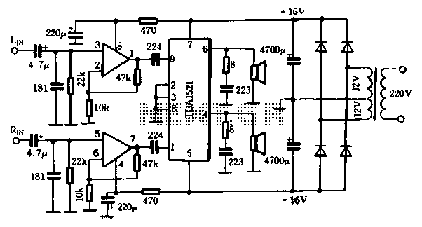
The first power amplifier circuit illustrated in Figure 5-88 utilizes the NE5532 operational amplifier, configured as a line amplifier, and features the TDA1521 power amplifier. This circuit operates with a dual power supply and eliminates the need for coupling...