
Attenuator circuit

The rectifier's bias current typically limits the gain reduction to approximately 70 dB. Resistor R16 enhances the rectifier's performance. After approximately 50 dB of attenuation, a slope of -6 dB/V is observed, with the slope increasing and the attenuation accelerating until the circuit is fully closed at around 9 V of control voltage. The operational amplifier should be characterized by low noise, high intensity, and fast scanning speed. Resistors R13 and R14 are configured to provide a 0 V bias to the output.
An exponential converter circuit utilizing an operational amplifier and transistors is designed to control gain effectively through a variable control voltage. The operational amplifier serves as the primary gain element, while transistors Q1 and Q2 facilitate the exponential conversion of the control signal into a corresponding gain control current.
The reference current of 150 pA is a critical parameter, establishing a baseline for the circuit's operation. With a supply voltage of 15 V and a resistor RZO of 100 kΩ, the initial gain is set. The design incorporates a logarithmic response to the control voltage, where each 1 V increase in the control voltage results in a 6 dB reduction in output gain, effectively doubling the attenuation for each increment. This characteristic allows for precise control over the output signal.
Capacitor C6 plays a vital role in stabilizing the circuit's response to changes in the control voltage. By introducing a time constant of 20 IDS, it mitigates abrupt fluctuations, ensuring that transitions in gain occur smoothly, thereby enhancing audio fidelity and reducing distortion during dynamic signal conditions.
Resistor R18 is strategically placed to ensure that the circuit reaches maximum attenuation, which is essential in applications where complete signal suppression is required. The rectifier's bias current, typically limiting gain reduction to around 70 dB, is managed by R16, which allows for enhanced performance and responsiveness of the rectifier circuit.
As the control voltage approaches 9 V, the circuit's attenuation increases significantly, achieving a rapid decline in output gain. This feature is critical in scenarios requiring swift response to control changes, making the design suitable for applications such as automatic gain control in audio processing systems.
The operational amplifier selected for this circuit must exhibit low noise characteristics, high output current capability, and fast response times to ensure optimal performance. Resistors R13 and R14 are utilized to maintain a 0 V bias at the output, further stabilizing the circuit and ensuring linear operation across the desired range of input signals. This arrangement is crucial for maintaining signal integrity in high-performance electronic applications.A op amp and transistors Q1 and Q2 exponential converter to generate an exponential gain control current, which is introduced into the rectifier. A reference current of 150 pA, (15 V and RZO = lOO-k), is attenuated by a factor of two (6 dB) for each increase of tension in the control voltage.
Capacitor C6 slows secure changes to a period of 20 IDS constant (C6 x IR) such that a sudden change in the control voltage will produce a gain change smooth sound. RI8 ensures that for control voltages of the circuit will go to great attentuation full. The rectifier bias current which would normally limit the gain reduction around 70 dB. RI6 attracts more courses of the rectifier. After about 50 dB of attentuation to -6 dB / V slope, with the increase in slope and the attenuation becomes much faster than the circuit to close completely at about 9 V control voltage. Al should be a low noise, high intensity, scanning speed, op. R13 and R14 in place around 0 V bias to the output.
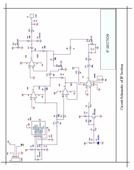
Related Circuits
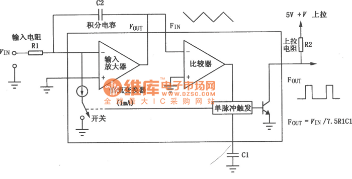
The VFC62 is a voltage-to-frequency and frequency-to-voltage converter that effectively transforms analog signals into digital signals. The digital output is presented in an open collector format, where the digital pulse repetition rate is directly proportional to the amplitude of...
Obtain more information about the circuit diagram of a mobile jammer by visiting this link. A GSM jammer, or cell phone jammer, is a device that transmits signals on the same frequency used by the GSM system. The effectiveness...
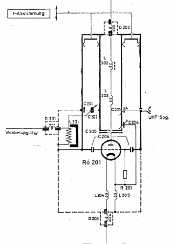
The use of a quarter-wave parallel-wire line as a tuning unit has been discussed in the chapter on Short Lines, where it was pointed out that these circuits have comparatively high Q even at higher frequencies. Their great length...
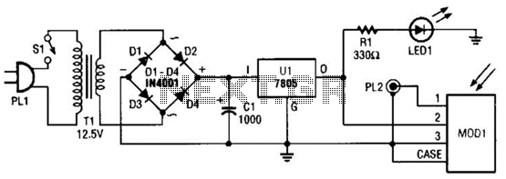
A schematic diagram for the remote analyzer is presented. The circuit is powered by a simple 5-V supply, which includes components such as PL1, SI, Tl, a bridge rectifier formed by diodes D1 through D4, capacitor CI, and a...
An LED, or Light Emitting Diode, is a semiconductor device that allows current to flow in one direction while blocking it in the opposite direction. This characteristic makes LEDs polarized components, having a positive side known as the anode...

A simple function generator that produces a specific frequency. While awaiting the arrival of the AD9832 chip, a basic version of a Direct Digital Synthesis (DDS) synthesizer was developed using only the AT2313 microcontroller and a resistor network. This...