
Audio compressor circuit

Long and short attack durations are managed by adjusting the values of Rx and R2. An emitter-follower Darlington configuration may be necessary if extremely slow decay times are required. The emitter-follower Q2 drives the AGC Pin 2 of the MC1590, effectively reducing the gain. Resistor R3 controls the slope of the signal compression.
The circuit configuration described utilizes a common emitter PNP transistor (MPS6517) as the primary amplification stage. This transistor is characterized by its ability to provide significant voltage gain, which in this case is set to approximately 20. The RL control mechanism is crucial for setting the quiescent point (biasing) of transistor Q, enabling the circuit to respond dynamically to varying input signal levels. The adjustment of the quiescent point ensures that the transistor operates efficiently within its linear region, allowing for optimal signal amplification.
Diode D1 plays a vital role in signal processing by rectifying the output from Q1, allowing only those positive signal peaks that surpass the threshold of approximately 7.0 volts to pass through. This rectification is essential for further processing the amplified signal, as it converts the AC signal into a pulsating DC signal that can be filtered.
The filtering stage, managed by resistor Rx, is responsible for determining the charging time constant, which directly influences the attack time of the circuit. Capacitor Cx is integral to this process, as it participates in both the charging and discharging cycles, affecting the overall response time of the amplifier.
Resistor R2, with a value of 150 K, acts as the input resistance for the emitter-follower Q2. This configuration is designed to provide a low output impedance while maintaining a high input impedance, which is beneficial for driving subsequent stages in the circuit. The decay time of the output signal is primarily controlled by R2, allowing for fine-tuning of how quickly the circuit responds to changes in input signal levels.
The circuit's design also accommodates the need for adjustable attack times, with the potential for long and short attack durations achieved through the careful selection of resistor values for Rx and R2. In scenarios where extremely slow decay times are desired, the implementation of an emitter-follower Darlington configuration may be warranted, as it provides enhanced current gain and improved performance in such applications.
The output stage, driven by emitter-follower Q2, interfaces with the AGC (Automatic Gain Control) Pin 2 of the MC1590, effectively managing the gain of the overall circuit. Resistor R3 is instrumental in controlling the slope of signal compression, allowing for further refinement of the output signal characteristics in response to varying input levels. This comprehensive design enables the circuit to adapt dynamically to different signal conditions, ensuring consistent performance across a range of applications.The amplifier drives the base of a common emitter PNP MPS6517 operating with a voltage gain of about 20. RL control varies the quiescent point of the transistor Q, so that varying amounts of signal exceed the level of V r, diode D 1 rectifies the positive peaks Ql output is only when these peaks are more larger than r V "'" 7.
0 volts. The result is filtered ex Rx. s, controls the charging time constant or time of attack. Cx is involved in two loading and unloading. R2 (150 K, the input resistance of the emitter-follower Q2) controls the decay time. Making the disintegration of long and short of attack is accomplished by small and large Rx R2. (An emitter follower Darlington may be necessary if the extremely slow decay times are required.) The emitter-follower Q2 drives the AGC Pin 2 of the MC1590 and reduces the gain. R3 controls the slope of signal compression.
Related Circuits
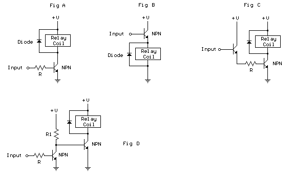
The schematic below illustrates four methods of controlling a relay with a digital logic signal. Figure A can be used in most cases where the relay coil requires 100 mA or less and the input current is 2 milliamps...
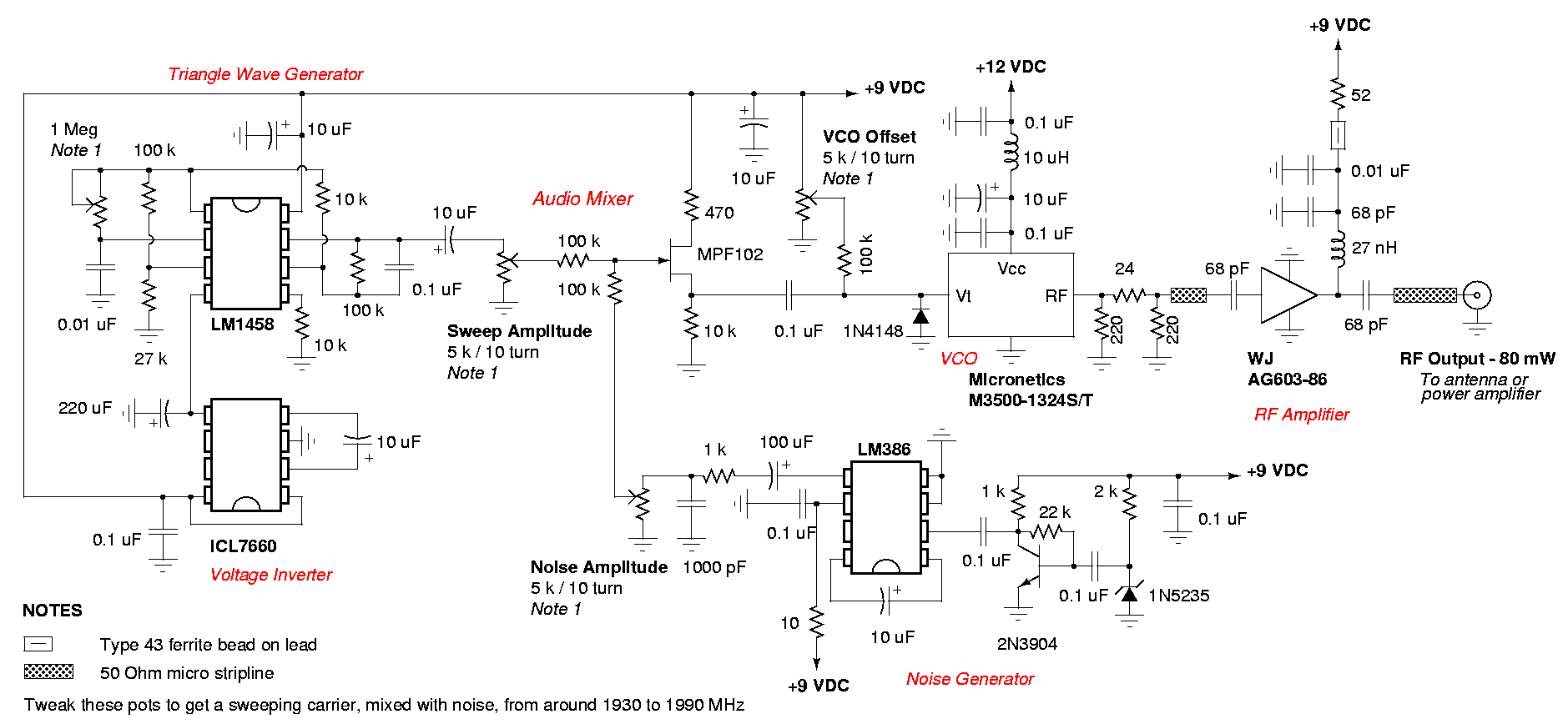
A DIY GSM jammer schematic diagram designed for use with GSM1900, operating within the frequency range of 1930 MHz to 1990 MHz. The GSM jammer circuit is intended to disrupt communication between mobile phones and base stations within the specified...
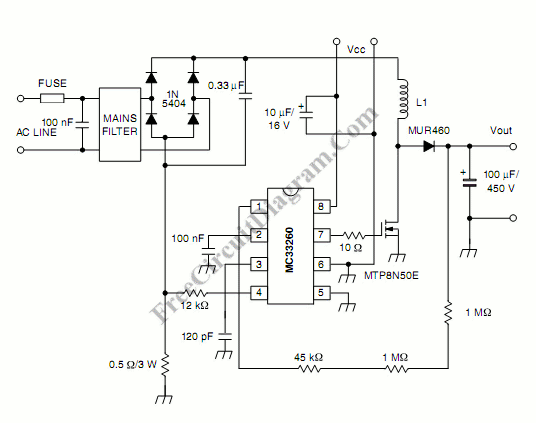
Active power factor correction stabilizes the electrical demand of a device to provide optimal power factor characteristics for various types of loads. To comply with power factor regulations, a cost-effective solution should be designed. In many applications, the requirement...

An alternative approach to utilizing operational amplifiers (op-amps) for power supply regulation is presented. This method necessitates an additional winding on the power transformer to provide the op-amps with a bipolar voltage of +/- 8 volts. The negative voltage...
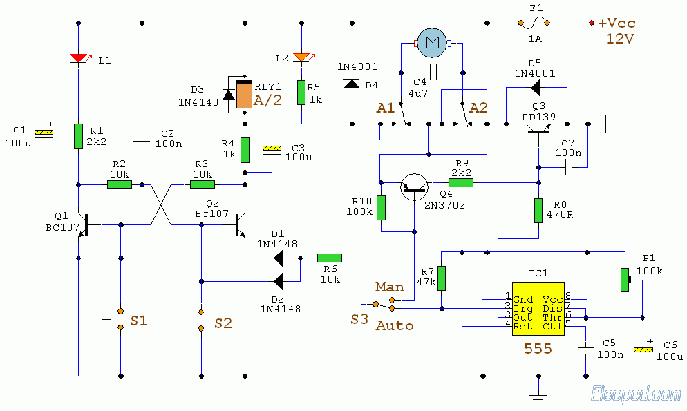
The following circuit illustrates a curtain control circuit diagram. This circuit is based on the 555 integrated circuit (IC). Features include a switch for manual control, the IC, and additional components. The curtain control circuit utilizes the 555 timer IC...
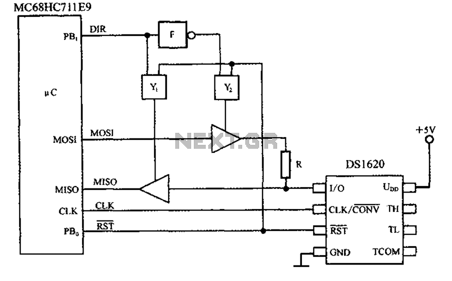
This circuit features a three-wire serial interface for smart temperature sensors, specifically the DS1620, along with an SPI bus interface circuit. The DS1620 is a high-accuracy digital temperature sensor that communicates over a three-wire interface, which consists of a data...