
Cell Phone Jammer Circuit

The GSM jammer circuit is intended to disrupt communication between mobile phones and base stations within the specified frequency range. The schematic typically includes a signal generator, an amplifier, and an antenna. The signal generator produces a noise signal that operates at the same frequency as the GSM1900 band. This noise signal is then amplified to ensure it has sufficient power to interfere with the communication signals.
The circuit may utilize components such as transistors or operational amplifiers to create the necessary gain and bandwidth. A bandpass filter can be included to ensure that only the relevant frequencies are amplified while rejecting out-of-band signals. The output is then fed to an antenna, which radiates the jamming signal over a specified area.
It is important to note that the use of GSM jammers is illegal in many jurisdictions due to their potential to disrupt legitimate communications, including emergency services. Therefore, this schematic should only be used for educational purposes and in compliance with local laws and regulations.A beautiful diy gsm jammer or mobile cell phone jammer schematic diagram for use only in GSM1900 with frequency from 1930 MHz to 1990 MHz. The GSM1900 mobi.. 🔗 External reference
Related Circuits
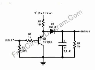
Using only a single transistor and a few passive components, a fairly sensitive peak detector circuit can be built. This peak detector circuit is suitable for various applications. The peak detector circuit utilizes a single transistor, typically configured in a...
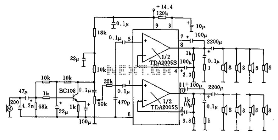
20W bus radio and megaphone circuit utilizing the TDA2005S double low-frequency power amplifier integrated circuit design. The front end can be connected to either a microphone input or a low-frequency radio output voltage amplification stage. Each TDA2005S provides 10W...
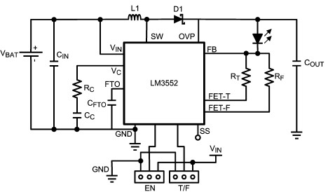
For this LED driver electronic project, a DC power supply circuit is required to provide an output voltage between 2.7V and 5.5V. The supply voltage must be applied between Vin and GND. The T/F jumper connects the T post...
Do not like your little brother's TV channel selection? Hate the volume your wife sets the stereo at? Want to just annoy someone? This circuit accomplishes all of that and more by jamming most infrared (IR) remote signals. The...
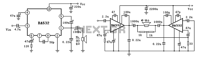
BA532 is a low-frequency power amplifier circuit designed for an output transformerless (OTL) application, capable of delivering up to 5.8W of output power. It features built-in protection against load short-circuits, over-voltage, and over-temperature conditions. The amplifier is housed in...
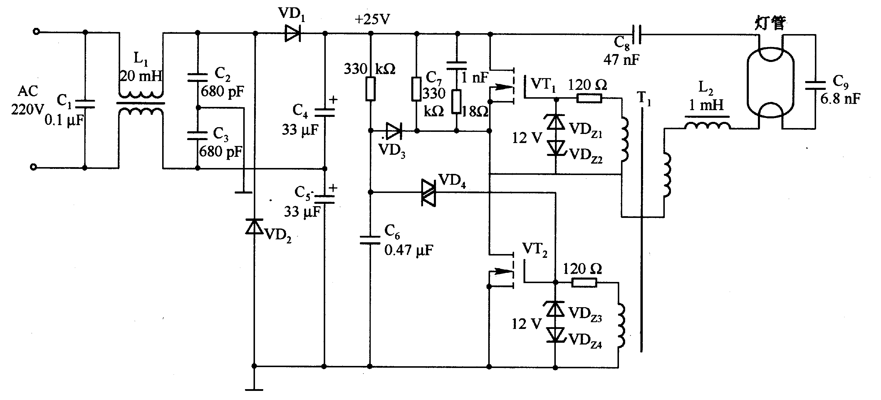
A fluorescent tube is connected in an LC resonant circuit consisting of inductor L2 and capacitor C9. The bidirectional breakdown diode VD4 initiates the starting circuit. When AC power is applied, the gate potential of transistor VT2 increases due...