
Audio Line Driver Circuit

The line driver circuit is designed to effectively transmit signals over low-impedance lines, making it suitable for various applications in audio and data communications. The core component, IC1, is selected for its low-noise characteristics, which are critical for maintaining signal integrity, especially in sensitive applications. The operational amplifier operates at a supply voltage of 15 V, ensuring adequate headroom for signal processing while minimizing distortion.
Voltage regulators T1 and T2 are essential for providing a stable power supply to IC1, which is crucial for consistent performance. These regulators ensure that fluctuations in the input voltage do not adversely affect the operation of the amplifier, thus enhancing reliability.
The output stage, consisting of transistors T3 and T4, is configured in a complementary manner, allowing for efficient drive capabilities. This configuration helps achieve higher output currents while maintaining thermal stability, which is vital when driving low-impedance loads. The complementary arrangement also aids in reducing crossover distortion, a common issue in linear amplifiers.
With a frequency response that remains flat up to 100 kHz, this line driver is well-suited for applications requiring high fidelity over a wide bandwidth. The ability to maintain a consistent gain across this frequency range ensures that the integrity of the signal is preserved, making it ideal for high-quality audio transmission and other precision applications. This line driver can drive low-impedance lines with up to 70 V p-p max. IC1 is a low-noise op amp suitable for 15-V operation. T1 and T2 are regulators for the power supply for IC1. T3 and T4 form a complementary power output stage. Frequency response is flat up to 100 kHz.
Related Circuits
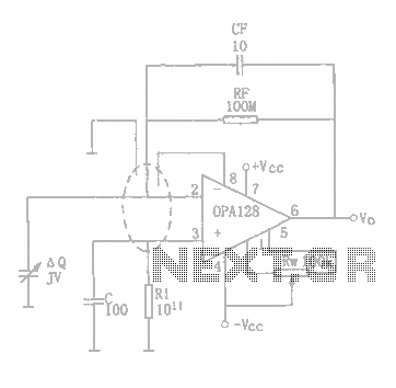
A charge amplifier is designed to amplify the signal charge from a piezoelectric device. It features a high internal impedance to accommodate the weak signal charge, which can be at the picoampere (pA) level. This necessitates a charge amplifier...
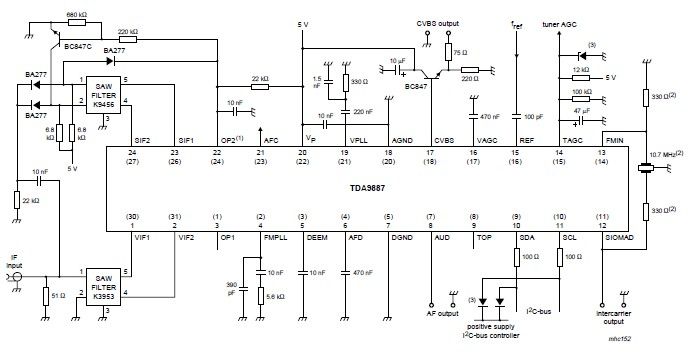
The integrated circuit (IC) is a multistandard vision and sound intermediate frequency (IF) phase-locked loop (PLL) demodulator that operates without the need for alignment. It supports multiple television standards, including PAL, SECAM, and NTSC, and is capable of handling...
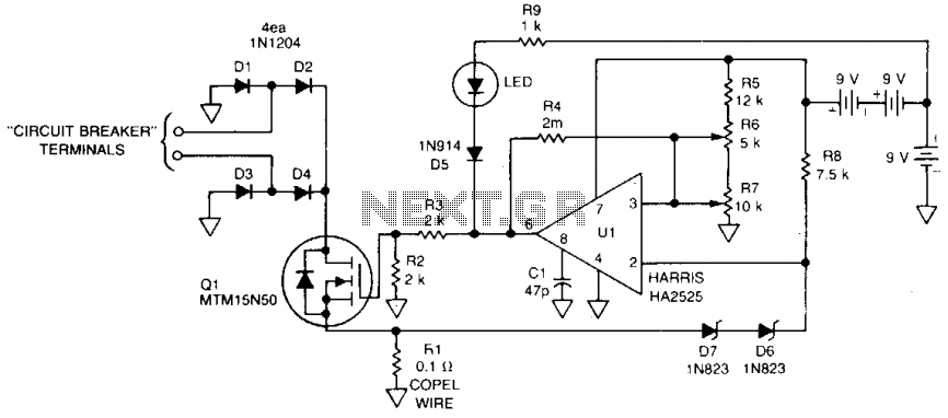
This 115 Vac electronic circuit breaker utilizes the low drive power, low on-resistance, and fast turn-off characteristics of the TMOS MTM15N50. The trip point is adjustable, and an LED fault indication is provided, with battery power ensuring complete circuit...
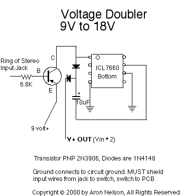
If you want to try a higher voltage with your pedals, try this simple and easy voltage doubler circuit which uses an ICL7660 CMOS Voltage Converter Chip. I have found that JFETs such as the J201 sound much better...
The digital scoreboard circuit is designed to display numerical values ranging from 0 to 9 on a common anode 7-segment display. The circuit employs a 7-segment driver integrated circuit (IC), specifically the 74LS47 or 74LS247. A 555 timer IC...

This touch-on switch can be activated through electrical means and can only be reset using a mechanical switch. When the touch terminal is activated by a finger, the SCR turns on and illuminates LED1. The circuit utilizes a silicon-controlled rectifier...