
Audio Mixer

The circuit features three distinct audio input channels, each managed by a potentiometer (R1, R2, R3) that allows for individual level adjustments. These potentiometers serve as variable resistors, providing control over the amplitude of the audio signals before they converge at the gate of the field-effect transistor (FET) Q1. The FET is utilized for its high input impedance and low output impedance characteristics, making it an ideal choice for audio signal processing.
Upon reaching the gate of Q1, the combined audio signals are amplified. The output from Q1 is then directed to the emitter-follower configuration formed by transistor Q2. This configuration serves to buffer the output, ensuring that the signal maintains its integrity while providing sufficient current drive to the subsequent stage, which is the external audio amplifier.
Capacitor C6 plays a critical role in this arrangement by blocking any direct current (DC) component in the output signal while allowing the alternating current (AC) audio signal to pass through. This ensures that only the audio frequency components are fed into the external amplifier, preventing any potential distortion or damage that could arise from DC levels.
Overall, this circuit design effectively combines multiple audio sources, allowing for flexible control over each channel's volume and ensuring a clean, amplified output suitable for further processing or amplification in an audio system. Three audio circuits are combined in the circuit shown. Each input is coupled to its own level potentiometer (Rl, R2, or R3) an d they are combined at the gate of FET Ql. The output of Ql is coupled to the external audio amplifier through emitter-follower Q2 and capacitor C6.
Related Circuits
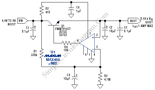
This low noise audio power supply circuit can reduce noise and ripple voltage by 40 dB over the 100 Hz to 20 kHz audio range. In portable applications such as... This low noise audio power supply circuit is designed to...
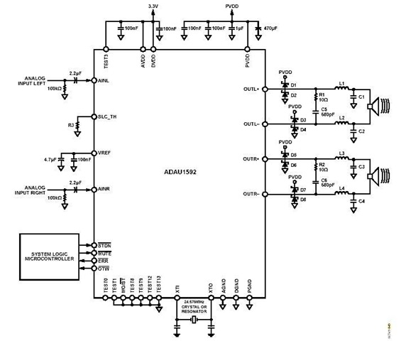
This is a stereo circuit schematic of the ADAU1592, a 2-channel, bridge-tied load (BTL) switching audio power amplifier. The ADAU1592 can be utilized in compact television sets, PC audio systems, and mini-component applications. According to the ADAU1592 datasheet, an...
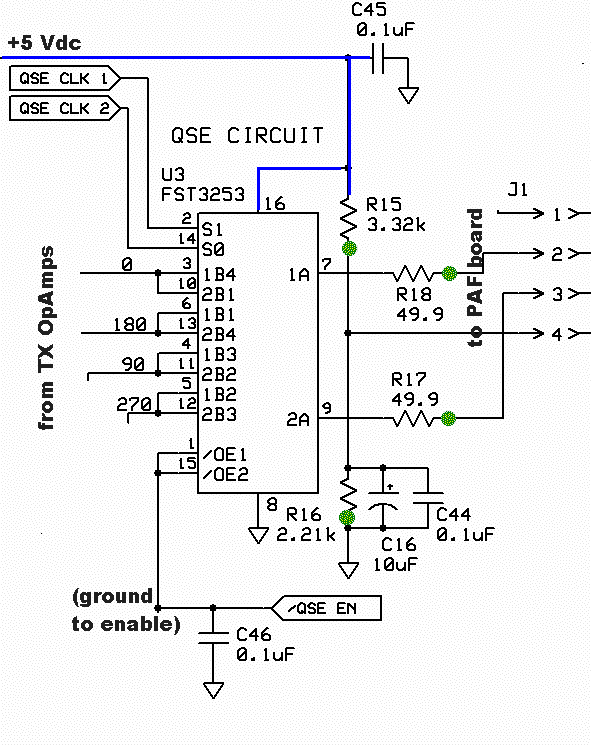
TX OpAmps TX Mixer (QSE) PTT RX Switching PA/Filters External Connections Comments Revisions WB5RVZ SDR Home. This stage integrates the TX Mixer into the board, allowing for the modulation of the Dividers' output signals by the four I and...
This circuit illustrates a Car Radio Audio Amplifier using the TDA2003 integrated circuit. The datasheet for the TDA2003 includes electrical characteristics and schematic wiring details. The TDA2003 is a high-performance audio amplifier designed for automotive applications. It is capable of...
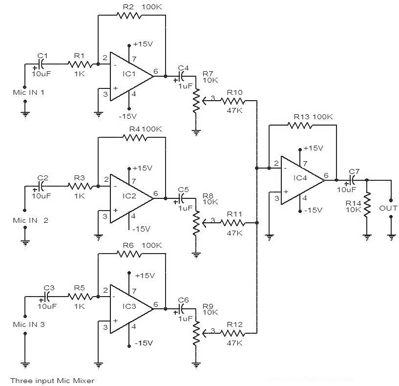
This is a circuit diagram of a 741 IC-based three-input microphone mixer circuit. A total of four 741 ICs are utilized, with IC1, IC2, and IC3 serving specific functions within the design. The circuit utilizes four operational amplifiers from the...

A 2 x 18W Hi-Fi Stereo Power Amplifier is designed using two TDA2030 integrated circuits (ICs). This amplifier features good input sensitivity, low distortion, stable operation, and comprehensive protection against overloads and output short-circuits. It can serve as a...