
100W HiFi Audio Amplifier Circuit
Technical specifications
Output power: 100W (RL = 4Ω, K = 0.1%) or 70W (RL = 8Ω, K = 0.1%) (continuous sinusoidal signal)
Power in relation to frequency: <10Hz-100KHz at 100W
Distortion: 0.1% at 20Hz-20KHz at 100W
Intrinsulation: 0.28% measured at 40Hz and 10KHz at a 4:1 ratio and Pa = 100W
Signal/Noise (SIN): 70 dB
Input sensitivity: 0.775V
Input resistance: 100KΩ
Output resistance: 0.052 Ω (at 1KHz)
Minimum load: 4Ω
Power supply: 80V symmetrical (+40V, 0, -40V)
Current consumption: 2.5A max at RL = 4Ω
Peak current: 50mA
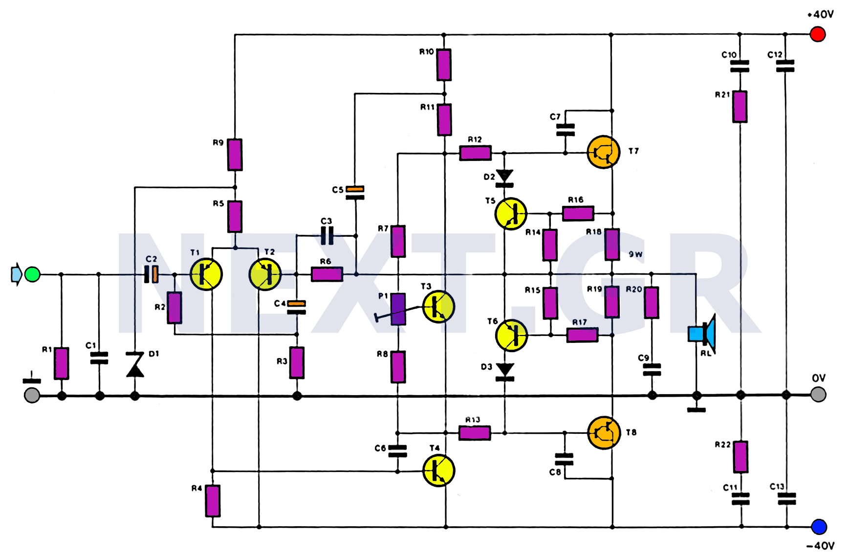
The circuit consists of a differential amplifier in the input stage, primarily utilizing transistors T1 and T2. A lead step is achieved with T4, whose collector connects to the emitter of T3, functioning as an adjustable Zener diode that regulates the resting current. The final output stage comprises two complementary Darlington transistors, T7 and T8. The symmetrical voltage design eliminates the need for electrolytic capacitors in the circuit.
The amplifier features a high input resistance exceeding 100KΩ, primarily due to the configuration of R2 and the high input resistance of T1. Negative feedback is implemented through resistance R6, which provides both DC and AC feedback. The DC feedback minimizes output potential, while the AC feedback determines amplification, dependent on R6, C4, and R3. The amplification can be calculated using the formula:
Uo/Ui = (R3 + R6)/R3 = 3420/120 = 28.5.
The T4 stage drives T7 and T8, which require minimal base current, negating the need for a heatsink for T4. Transistor T3, along with resistors R18 and R19, stabilizes the output current of the output transistors. The voltage drop across R18 and R19, controlled by P1, dictates the collector voltage from the T3 emitter. R11, in conjunction with capacitor C5, enhances the AC boost of the drive.
The output stage is centered on the Darlington transistors BDX66 and BDX67, which at 25°C exhibit the following characteristics: collector voltage of 100V, maximum collector current of 16A, and maximum power absorption of 150W. When the collector current reaches 10A, the collector voltage from the emitter is approximately 2V, yielding a DC amplification of about 1000. At a collector current of 5A, the voltage ranges from 0.4V to 0.5V, resulting in an amplification of around 4000. These transistors are well-suited for this application, but protection from short circuits is essential.
The voltage drop across the collector resistors R18 and R19 indicates the magnitude of the collector current through the transistor. If this current exceeds a certain threshold, it activates transistors T5 and T6, reducing the base currents of T7 and T8, thereby lowering the collector currents.
Additional components such as capacitors and resistors serve various functions. Capacitor C1 limits the input bandwidth to mitigate noise, while C3 is responsible for a 3dB point at 100KHz, influencing the frequency response characteristic. Capacitors C6, C7, and C8 function as Miller capacitances, and C9 and R20 stabilize the output. Capacitors C10, R21, C12, C11, R22, and C13 help eliminate RF frequency peaks from the power supply.
The construction of the circuit is straightforward, and with optimal conditions, the amplifier can deliver 120W at 4Ω, although distortion may reach about 1%. At 100W (again at 4Ω), distortion remains below 0.1%. The performance characteristics indicate that distortion stays consistent and below 0.1% across frequencies from 40Hz to 20KHz, with an input requirement of greater than 0.775V, which is standard for most preamplifiers. A 10KΩ potentiometer may be necessary for higher output devices at the amplifier's input.
The amplifier requires a symmetrical voltage supply of ±40V. At full power (100W at 4Ω), the current is 2.5A, while at an 8Ω load with 70W, the current is 1.1A. A non-stabilized power supply is recommended for simplicity and cost-effectiveness, although it may exhibit voltage fluctuations. The design must ensure that the maximum operating voltage of the output elements, rated at 100V (±50V), is not exceeded. Therefore, a supply voltage of ±46V is suggested to provide a safety margin.
Construction guidelines specify that resistors R18 and R19 must maintain a PCB spacing of at least 5mm for effective heat dissipation. Transistors T7 and T8, along with capacitors C7 and C8, should be mounted on a heatsink with a thermal resistance of 1.2°C/W. If thermal paste is applied, a heatsink with 1.8°C/W is adequate. Direct contact between the transistors and heatsink is prohibited to avoid short circuits, necessitating the use of insulators such as mica.
The input jack should connect to an AF cable on the printed circuit board, with coaxial cables grounded. The ground connection should be made as far from other components as possible to reduce noise interference. The secondary windings of the transformer must be entirely separate, leading to four wires that need to be connected appropriately based on voltage measurements.
Adjustment procedures involve short-circuiting the input and ensuring the output is disconnected before monitoring the current through the fuse block with a multimeter. The potentiometer should be adjusted to achieve the desired resting current in the power transistors.
A comprehensive list of components for both the amplifier and power supply is provided, detailing resistors, capacitors, semiconductors, and other necessary elements for construction and operation.This Amplifier was designed to have the following specifications: Distortion less than 0.1% at full power of 100W even at 20KHz. Power has to be attributed to an extended bandwidth. The output transistors must be protected against short circuits. The power supply must be symmetrical so that no electrolytic capacitors are needed at the outlet. Enhancer materials must be common and accessible to everyone. Construction and adjustment must be simple. The amplifier must be economical and efficient. The whole circuit is based on two Darlington output transistors that with the help of the input circuits give almost perfect results.
Technical specifications
Output power: 100W (RL = 4Ω, K = 0.1%) or 70W (RL = 8Ω, K = 0.1%) (continuous sinusoidal signal)
Power in relation to frequency: <10Hz-100KHz at 100W
Distortion: 0.1% at 20Hz-20KHz at 100W
Intrinsulation: 0.28% measured at 40Hz and 10KHz at a 4: 1 ratio and Pa = 100W
Signal/Noise (SIN): 70 dB
Input sensitivity: 0.775V
Input resistance: 100KΩ
Output resistance: 0.052 Ω (in 1KHz)
Minimum load: 4Ω
Power supply: 80V symmetrical (+ 40V, 0, -40V)
Current consumption: 2.5A max at RL = 4Ω
Peak current: 50mA
The circuit
The input stage, is a differential amplifier with main elements the transistors T1 and T2. Then we have a lead step with T4 whose collector is connected to the T3 emitter. This works like an adjustable Zener diode and regulates the resting current. The final step follows with two completely complementary transistors T7 and T8 (Darlington).
An advantage of the symmetrical voltage, is that the electrolytic capacitor is avoided at the circuit.
The amplifier has a fairly high input resistance that exceeds 100KΩ since before C4 we have R2, and since the input resistance of T1 is too high.
Negative feedback (both for DC and for AC) we have with resistance R6.
The DC negative feedback section produces almost zero potential at the output. The feedback section AC determines the amplification and is dependent on R6, C4 and R3. The amplification is determined by the formula:
Uo/Ui = (R3 + R6)/R3 = 3420/120 = 28.5
The stage with T4 leads the T7 and T8, but because they are darlington they need very little base current, so for T4 we do not need a heatsink.
Transistor T3 together with resistors R18 and R19 stabilizes the output current of the output transistors. The voltage drop on R18 and R19 is determined by the position of P1 because it controls the collector voltage from the T3 transmitter.
R11 in conjunction with C5 capacitor increases the AC boost of the drive.
The heart of the output stage is the Darlington transistors BDX66 and BDX67. At 25°C this series has the following characteristics:
- • Collector collector voltage: 100V
- • Max Collector Current: 16A
- • Maximum power absorbed: 150W
If the collector current becomes 10A then the collector voltage from the transmitter becomes 2V and the amplification at DC is about 1000.
When the collector current is 5A then the voltage is between 0.4V and 0.5V and the amplification is about 4000.
With these characteristics these transistors are ideal for such circuits. Regardless of how "good" the transistors are, they need protection from short circuits.
The voltage drop on the collector resistors R18 and R19 gives us the magnitude of the collector current through the transmitter.
If the current passing through the resistors R18 and R19 passes a certain limit, then they will start to drive the transistors T5 and T6 since the voltage on the dividers R16, R14 and R15, R17 parallel to R18 and R19. Thus the currents passing through the diodes D2 and D3 will reduce the base currents of T7 and T6, which will also reduce the collector currents.
The various other elements R and C serve different purposes.
C1 limits the input bandwidth. This avoids a portion of noise. C3 is responsible for 3dB at 100KHz, that is to say, it is inclined to the characteristic of the frequency response. C6, C7 and C8 are Miller capacities. C9 and R20 stabilize the output. The C10 / R21, C12, C11 / R22 and C13 cut off the various peaks at the RF frequencies coming from the power supply.
Technical specifications
The circuit has no difficulty and its construction is relatively easy.
With some luck, the amplifier can give 120W of power at 4Ω, but unfortunately the deformation reaches about 1%. But at 100W (again at 4Ω) the deformation is less than 0.1%.
From the following figure we see that the deformation remains constant and is less than 0.1% at frequencies from 40Hz to 20KHz.
For full performance the input must be greater than 0.775V. This level is given by almost all preamplifiers. If a higher output device is used then a 10KΩ potentiometer must be fitted at the input of the amplifier.

The power supply
It is known that the performance of the amplifier depends on the quality of the power supply. The amplifier needs a symmetrical voltage of ± 40V. At full power (100W at 4Ω) the current is 2.5A and at load 8Ω with power 70W the current is 1.1A.
For economy and simplicity, we use a non-stabilized power supply. By its nature, however, such a power supply will have a fluctuation in voltage.
If the power supply at full power output is 40V it means that with less power the supply voltage will tend to increase. However, since the output elements have a maximum operating voltage of 100V, which means ± 50V, the design should be done so that these limits are not exceeded.
For this reason, we define the power supply voltage to ± 46V so that we also have a safety margin. However, the ± 46V only leaves a margin of 6V between maximum and minimum load. However, this means that the internal resistance of the power supply must be very small. A good way to get a little resistance is to use a good transformer.
Given the good transformer, a bridge-rectifying bridge and some electrolytic capacitors and we have the power supply we need.
The fuses on each power line are used to protect the circuit from short circuits, because the T7 and T8 protection circuits are only short-lived until the fuses are blown. For stereo performance we need two amplifiers and therefore two power supplies.
Construction
Resistors R18 and R19 must have a PCB spacing of at least 5mm.
This generates a good bleed and hence good heat dissipation. Transistors T7 and T8 as well as capacitors C7 and C8 are mounted on the heatsink.
The heatsink must be 1.2 ° C / W. If a heat-conducting paste is applied on both sides, then a heatsink with 1.8 ° C / W is sufficient.
It is known that if more than one transistor is placed on a heatsink then we have to divide the thermal resistance of the heatsink with the number of transistors. Therefore, if both transistors (T7 and T8) are placed on a heatsink, then the type should be 0.6 ° C / W or 0.9 ° C / W.
In no case should there be direct contact of the transistor with the heatsink, because the collector is connected to the transistor cover and thus would cause short circuits.
For this reason, insulators such as, for example, Mica.
Before connecting the capacitors C7 and C8 (see Fig. 4), insulate their terminals by placing eg. Plastic macaroni.
The connections to the printed circuit must be made with the shortest possible copper wire.
The input jack must be connected to an AF cable in the printed circuit (coaxial cable should be grounded).
The best way to connect the ground to the amp printed box is to ground the input jack. The cable and the plug must be positioned as far as possible from the other components and cables to reduce the possibility of back-up and noise from the 220V network.
The two windings of the secondary are completely separate. That means four wires will remain in our hands. To see where we connect each one we get two in luck and unite them. Then we measure the voltage in the other two. If the voltage between them is 60V AC, then connect the two wires together with the earth of the power supply and the other two in the remaining free points.
If the voltage is 0V, then we need to change one of the edges we've joined with a free one. Electrolytic capacitors must be attached (due to size) to the PCB with a plastic collar or the like.

Adjusting the amplifier
Remove F2 from the power supply after short-circuiting the input and making sure the output is not connected to anything else. Then put a multimeter in the 1A DC region at the ends of the fuse block, and with the (+) in its side with C2.
Turn the potentiometer to its end in a direction opposite to the clock.
Check all connections and connect the power adapter to the network. The multimeter should point around 0A. If the reading is greater then an error must be present and you must immediately stop the power supply. In good condition the current should be about 100mA which with P1 must be set to 80mA. This means that the resting current in the power transistors will be about 50mA.
This is the whole process of adjusting the amplifier.
We replace F2 fuse, after first shutting down the power supply. If an error has occurred, we can easily correct it by comparing the voltages at different points in the circuit. These voltages have been measured with the speaker connected and the input disconnected.
List of amplifier components
Resistors:
R1 = 120k | R2,R5,R6 = 3k3 | R3 = 120Ω | R4,R8 = 680Ω | R7 = 1k5 | R9 = 5k6 | Α10 = 1k2 | R11 = 2k7 | R12,R13 = 270Ω | R14,R15 = 15Ω | R16,R17 = 220Ω | R18,R19 = 1Ω/9W | R20 = 10Ω | R21,R22 = 1Ω | Ρ1 = 1k
Capacitors:
C1 = 470 pF | C2 = 10μF/63V | C3 = 150pF | C4 = 1000μ/4V | C5 = 220μ/40V | C6 = 47pF | C7,C8 = 560pF | C9 = 47nF | C10,C11 = 680nF | C12,C13 = 100nF
Semiconductors:
Τ1,Τ2 = BC556Α | Τ3,Τ5 = BC547B | Τ4 = BC639 | Τ6 = BC557B | Τ7 = BDX67B,BDX67C | Τ8 = BDX66B,BDX66C | D1 = 9V1/1.3W | D2,D3 = 1Ν4148,1Ν914,BAW62
Other:
2 heatsinks 1.2 ° C / W or 1.8 ° C / W (see text) | Insulators for power transistors (mica)
List of power supply components
Resistors:
R1, R2 = 3k3 / 1W
Capacitors:
C1 = 100nF | C2, C3 = 4700μF / 63V
Semiconductors:
D1, D2 = LED | B1 = B80C 3200/5000 Rectifier (Bridge)
Fusses:
F1 = 1.4A (approx.) | F2, F3 = 2.5A (approximately)
Other:
Toroidal transformer = Secondary 2 x 30V - 2x 3,75A | S1 = bipolar switch | Two fuses for PCB | A fuse box for 220V
Related Circuits
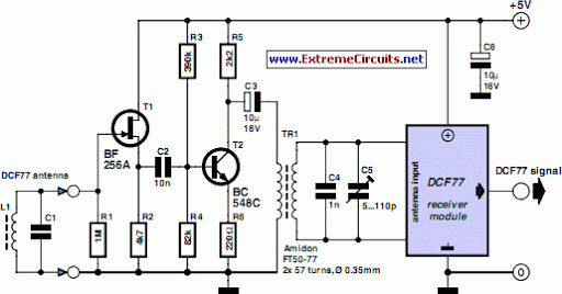
A popular project among microcontroller enthusiasts is to build a radio-controlled clock. Tiny receiver boards are available, featuring a pre-adjusted ferrite. The radio-controlled clock project leverages a microcontroller to receive time signals transmitted from a time signal transmitter, typically operated...
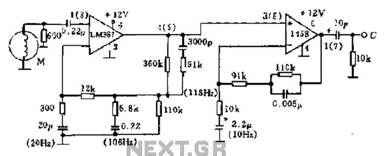
The phonograph pickup head is represented in the schematic as component M, which generates the pick-up signal and is processed through an LM387 amplifier circuit. The LM387 is part of the LM38X series, recognized for its advanced linear amplifier...
For example, I do not understand the process of demodulation or the modulation itself, and so on. Is there someone who can understand this circuit? Could you please assist me? The circuit in question likely involves a modulation and demodulation...
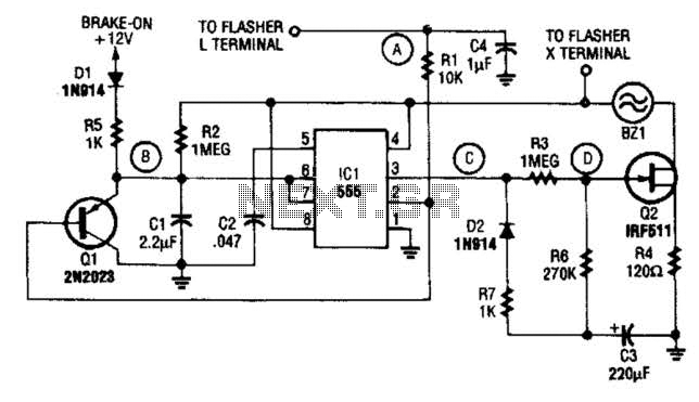
The STS schematic illustrates a circuit designed to alert a driver when the turn signal has been active for more than 15 seconds. The voltage at the gate of transistor Q2 increases in response to the charge accumulated on...
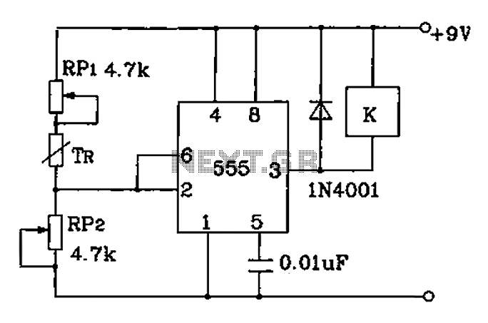
Adjust RP1 and RP2 to set the preset temperature control point. The 555 circuit is configured as a Schmitt inverter circuit that automatically controls a relay device. This forms part of the T-121 temperature control circuit, which includes a...
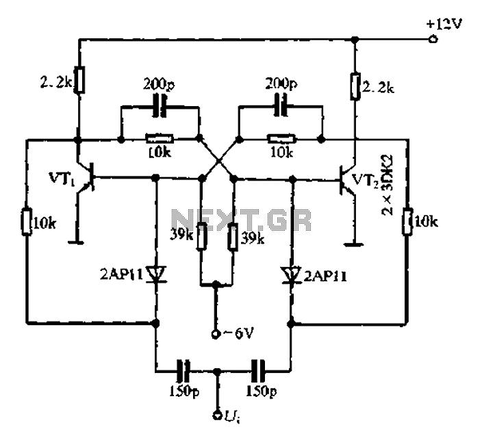
Bistable circuit operating at a frequency of 100 kHz or less. A bistable circuit, also known as a flip-flop, is a type of electronic circuit that has two stable states and can be used to store binary information. This circuit...