
walkie talkie circuit research project

The circuit in question likely involves a modulation and demodulation process, which is essential in communication systems for transmitting information over various media. Modulation refers to the technique of varying a carrier signal's properties, such as amplitude, frequency, or phase, to encode the information being sent. Common modulation techniques include Amplitude Modulation (AM), Frequency Modulation (FM), and Phase Modulation (PM).
Demodulation is the reverse process, where the modulated signal is converted back into its original form for interpretation. This process typically involves filtering, amplification, and signal detection to retrieve the encoded information. The circuit may include components such as mixers, filters, amplifiers, and demodulators tailored to the specific modulation technique used.
A detailed understanding of the circuit's schematic is crucial for grasping the modulation and demodulation processes. Key components to examine include the input signal source, the modulator stage, which shapes the carrier signal based on the input, and the demodulator stage, which extracts the original signal from the modulated carrier. Additionally, analyzing the power supply, grounding, and signal paths within the circuit can provide insights into its operation and performance.
To gain a better understanding, it may be beneficial to study the specific type of modulation employed, the frequency ranges involved, and the intended application of the circuit. This knowledge will facilitate a clearer comprehension of how the circuit functions overall and the role each component plays in the modulation and demodulation processes.for example i dont get the way the demodulation is done or the modulation itself an so on please is someone able to understand this circuit could you give me a hand 🔗 External reference
Related Circuits
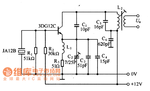
The 27MHz quartz crystal oscillator circuit is illustrated in figure 1. The biasing circuit consists of resistors R1, R2, and R3, while C6 serves as the bypass capacitor. The partial voltage circuit includes capacitors C1, C2, C3, and C4...
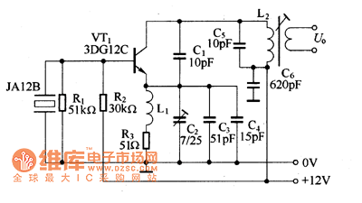
The 27MHz crystal oscillator circuit is illustrated in the figure. Resistors R1, R2, and R3 serve as biasing resistors, while capacitor C6 functions as a bypass capacitor. The voltage division circuit consists of capacitors C1, C3, C4, and C2,...
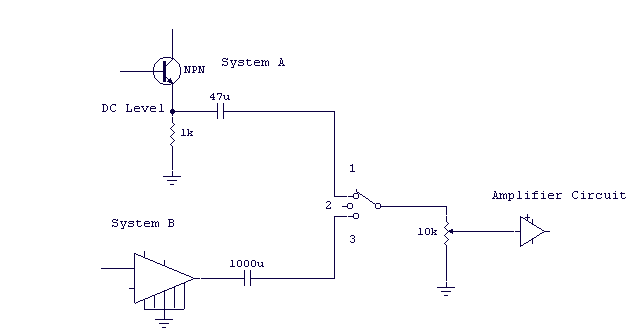
You may be familiar with this effect. You switch audio equipment such as an amplifier to a different input and there is a loud click or "thump" in the speaker system. Not all equipment is affected. Some high-end audio...
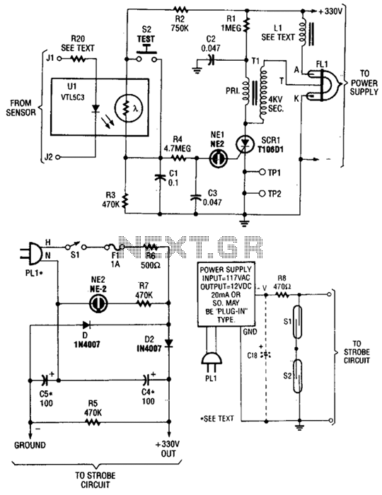
The circuit is activated by an LED/photoresistor isolator (U1), which combines a light-dependent resistor (LDR) and an LED in a single package. This device was selected for its high isolation characteristic of 2000 V, which is essential since the...
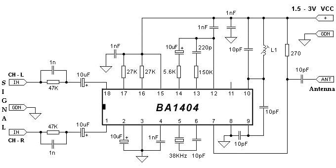
The BA1404 can be utilized to create a simple and effective FM stereo modulator electronic project. This BA1404 FM stereo modulator device operates within the FM broadcast band (75-108 MHz) and requires only a few common external components. The...
In the event of a sudden power failure in an elevator, it is crucial for the duty officer in the distribution room to be alerted promptly to prevent panic among passengers trapped inside. The following describes a sound alarm...