
TA-1500 fever amplifier circuit

The described circuit consists of several key sections that work together to achieve high-quality audio amplification. The front tone circuit is designed to manipulate the audio signal's frequency response, allowing for adjustments in treble, midrange, and bass frequencies. The operational amplifier configuration ensures that the microphone signal is effectively amplified, providing a clear input for further processing.
The pre-phono input circuit (IC3) serves to prepare the audio signal for amplification, ensuring that it is at an appropriate level for the subsequent stages. This section is crucial for maintaining signal integrity and preventing distortion.
The final amplifier stage is a Class A design, known for its linearity and low distortion characteristics. This amplifier utilizes a fully symmetrical design, which helps in balancing the output and reducing any potential noise. The complementary differential amplifier configuration enhances the circuit's performance by improving the common mode rejection ratio, which is essential for maintaining audio fidelity in the presence of noise.
The output stage, driven by VT18 and VT20, is designed to provide sufficient power while minimizing distortion. The coincident bias circuit ensures that the output transistors operate efficiently, maintaining a low output resistance that is vital for driving the load effectively. The heat sink mounted on key transistors provides thermal stability, preventing overheating and ensuring reliable operation.
The overall design emphasizes the importance of component selection and circuit layout, as these factors significantly influence the sound quality and performance of the amplifier. The adjustments provided by VR3, PR1, PR3, and PR8 allow for fine-tuning of the audio output, accommodating various signal sources and listening preferences. This comprehensive approach to design and functionality ensures that the final product meets high standards of audio performance.(Only shown the R channel, the original reference PCB label) o Figure (a) for the front tone circuit. The RC circuit genus common negative feedback operational amplifier. Microphone signal amplification by VTz after the VR3 fed ici negative input signal is mixed with the main station after the 1C1 O pin output o PR1, PR3, respectively, to control the main signal, the volume of the microphone signal to accommodate different signal sources. Tone negative feedback network Yizhu common type, high, medium and bass respectively adjusted, the principle is omitted.
Figure (b) is an independent pre-phono input circuit IC3 and balanced network structure, the actual installed capacity of the heart, as the need to decide FIG. (C) for the final amplifier circuit. This is typical of the new Class A dynamic bias fully symmetrical amplifier. This is a class with a fever the level of the final amplifier. Proper component selection, correct installation and commissioning, the sound quality is quite capable of satisfying.
VT4.VT6 VT8, fully symmetrical mirror VT10 constitute complementary differential amplifier circuit has a very high common mode rejection ratio and a wide dynamic range of port VT12.VT14 are cleverly connected across the two outputs of the differential circuit to further improve the signal to noise ratio and dynamic circuit voltage symmetrical form a full range oVT18.VT20 drive class. Power output from the VT22, VT26 complete O RP8.VT16, VT24 coincident bias circuit, with its low output resistance, so drive class VT18, VT20 base AC voltage drop close to zero; PR8 for adjusting the VT24 Vce to control end-stage stationary Harcourt current, final work in a dynamic state of the CPI.
VT24 and VT22, VT26 with mounted on a heat sink for temperature compensation tracking 6 adjusted VR7 make the whole circuit midpoint Paul held at zero potential to accommodate discrete transistors and power fluctuations mouth
Related Circuits
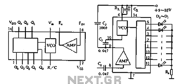
The circuit shown is a lighting control circuit that adjusts the speed of the flash output based on the strength of an audio signal. It utilizes eight flash integrated circuits (ICs) of the type LP188, which is housed in...
When the amplifier is installed inside the suitcase, it will require a change to stop working. The LA47536 has a control pin (pin 4) that requires a small voltage of up to 2V to turn on the amplifier. Transistors...
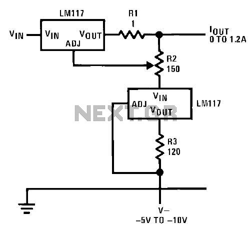
This circuit illustrates an adjustable regulator configuration that incorporates a voltage regulator. In this design, the LM117 regulator is utilized instead of the LM113 diode for reference. Both regulators necessitate a negative supply to function correctly with respect to...
In this circuit, two 567 tone decoders are utilized. One functions as an oscillator, while the other acts as a detector. Connecting TP1 and TP2 allows U2 to receive the signal from U1, resulting in pin 8 of U2...
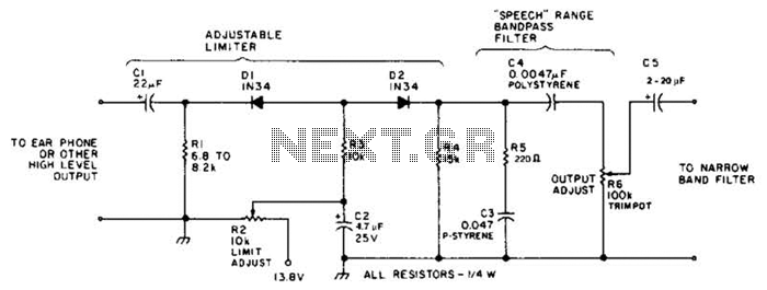
This circuit employs a diode series clipper to limit noise peaks on a received signal. It is most effective in scenarios where several volts peak-to-peak of audio signal are present. The diode series clipper circuit is designed to protect subsequent...
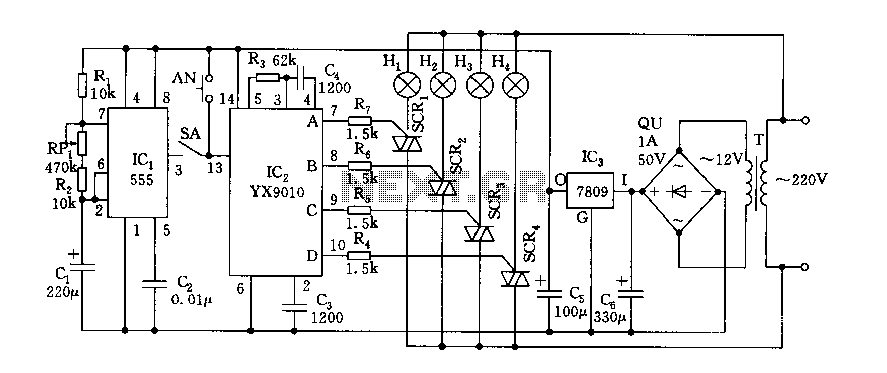
Fantasy lights offer wonderful changes suitable for storage, dance halls, or family holiday decorations. The control circuit is depicted here, which includes a multivibrator control circuit, a thyristor trigger circuit, and a step-down power supply circuit. The AC step-down...