
Automatic Muting Circuit For Audio Systems PCB

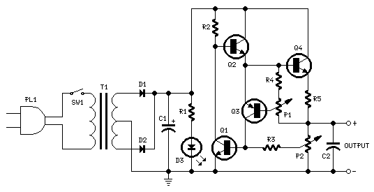
The automatic muting circuit described is designed to enhance audio systems by preventing unwanted noise during silent periods. The core component, the LB1403, acts as a comparator that monitors the audio signal level. When the audio signal from the pre-amplifier drops below the defined threshold, the circuit ensures that the output remains active, allowing the audio to pass through without interruption. The variable resistor VR1 allows for fine-tuning of the input signal gain, which is crucial for achieving optimal performance across various audio sources.
Transistor T1, a BC548, operates as a switching device that responds to the input signal from the pre-amplifier. The output from the LB1403's comparator is used to control transistor T2, which serves as the muting switch. When the audio input exceeds the threshold, T2 is activated, resulting in the muting of the audio signal by pulling the output at point A close to 0V. This effectively silences the audio output, preventing any unwanted noise from being transmitted to the amplifier.
Capacitor C4 plays a significant role in determining the muting delay period. By adjusting its capacitance, the designer can control how quickly the muting action occurs when the audio signal falls below the threshold. This delay can help to avoid abrupt audio cut-offs, providing a smoother listening experience.
For compatibility with STK series amplifiers, additional circuitry may be required to adapt the muting function to the specific needs of these devices, particularly regarding the negative voltage requirement for muting. The modifications ensure that the circuit functions correctly within the operational parameters of the STK amplifiers, maintaining the integrity of the audio signal while providing the necessary muting capabilities.Here`s a circuit diagram of automatic muting for audio systems using IC LB1403. The signal from pre-amplifier such as LA3160, LA3161 or HA1032 is connected to the base of the amplifier transistor BC548 (T1). Variable resistor VR1 is used to control the gain of input signal. Comparator 2 output at pin 2 of LB1403 is used for generation of muting s ignal at the emitter (point A) of transistor T2, which can be directly connected to muting pin 4 of amplifier employing IC LA4440. As long as the audio input to the circuit of Fig. 1 is below a certain level (say, 150 mV peak to peak), the output at point A will be high. Once the input crosses this threshold level, the output will be around 0V. Capacitor C4 determines the on`/off` muting delay. Higher the value of this capacitor, greater will be the muting delay period. Slight circuit modification will be needed if this circuit is used with STK series amplifiers, such as STK 4141, 4142, 4152, and 4191, because they need negative polarity voltage for muting.
The additional circuit to be connected at point A in that case is shown in Fig. 2. 🔗 External reference
Related Circuits
A Variable DC Power Supply is an essential tool for electronics hobbyists. This circuit is not entirely new, but it is simple, reliable, robust, and short-proof, offering variable voltage up to 24V and variable current limiting up to 2A....
Assistance is needed to understand a schematic. Most components are clear, except for the triangular symbols which are likely operational amplifiers (op-amps). Clarification is required on their implementation and arrangement. The current diagram is intended for testing with a...
The AP500A amplifier offers numerous advantages, providing unmatched superiority in stereo applications. It can utilize various amplifier configurations, including OTI, CI, rK, BTL, class AB, and super CP. The typical DC amplifier module for the AP500A is illustrated in...
Connect a 12V fan to this circuit that consumes 70mA (0.07A), ensuring the circuit can supply at least that amount of current. There appears to be a misunderstanding regarding the analysis. The voltage drop across the resistor equals the...

An average ability amplifier characterized by acceptable overall quality, while being simple in construction. It is frequently used in live loudspeakers. The design incorporates high-quality FET transistors, specifically HEXFET technology, which are voltage-controlled rather than conventional bipolar transistors. The...

The ptPC1891A application circuit features a working state switch (SA) with a total of four options. It primarily utilizes ICs 11 and 12 to set different logical levels, as referenced in Table 5-12. The high level is denoted as...