
Autopatch telephone line interface

The described circuit connects a receiver to a phone line and a phone line to a transmitter, ensuring effective signal transmission and reception. The operational amplifier plays a critical role in this configuration, providing necessary gain to the signals being processed.
In this application, the op-amp is typically configured in a non-inverting mode to amplify the weak signals received from the transducer or sensor. The input from the receiver is fed into the non-inverting terminal of the op-amp, while the output is taken from the op-amp's output terminal, which then connects to the phone line. The gain of the op-amp can be adjusted using feedback resistors, allowing for optimal signal strength based on the specific requirements of the communication system.
For the phone line to transmitter link, a similar configuration can be employed. The output from the phone line can be fed into another op-amp stage, which ensures that the signal is sufficiently amplified before it reaches the transmitter. This stage is crucial for maintaining the integrity of the signal over longer distances, minimizing the effects of noise and attenuation that may occur along the transmission path.
In addition to the op-amps, the circuit may also include passive components such as resistors and capacitors for filtering and stability purposes. Properly designed power supply circuitry is essential to ensure that the op-amps operate within their specified voltage range, which is critical for maintaining performance and preventing distortion.
Overall, this circuit design effectively enables communication between various components in a telecommunication system, leveraging the capabilities of operational amplifiers to enhance signal quality and reliability.This circuit provides for the receiver-to-phone line and phone line-to-transmitter link with both using an op amp for gain.
Related Circuits
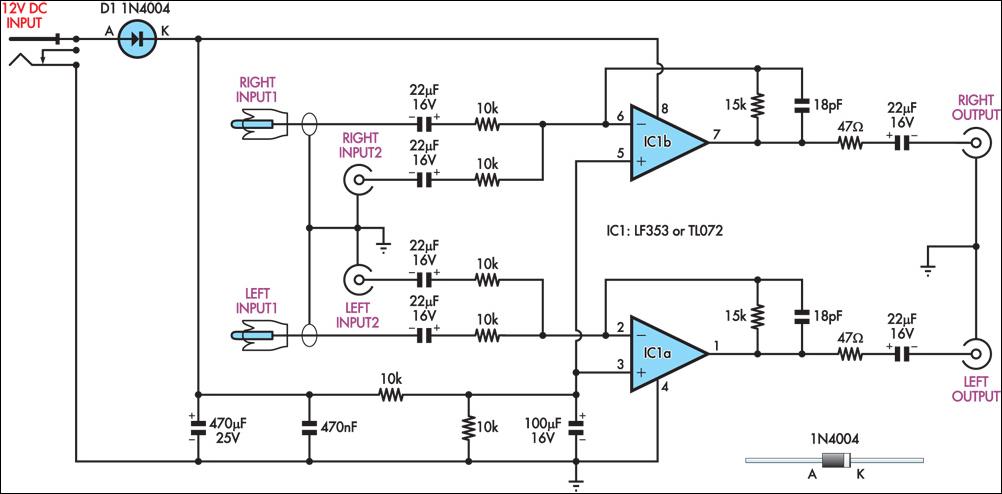
This circuit combines two separate line-level stereo (L & R) signals into one stereo (L & R) output, eliminating the need to switch between two pairs of input signals. It is utilized in a scenario where the stereo audio...
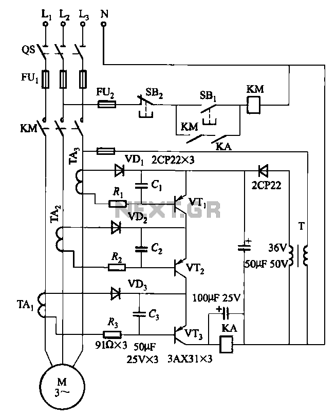
Drawing transistors that comprise the gate VTi, VT2, VT3, and similar components. The schematic involves a configuration of transistors designated as VTi, VT2, and VT3, which are integral to forming a gate structure. These transistors are typically arranged in a...
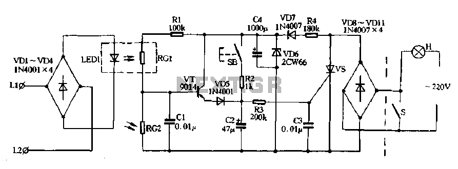
Diodes VD8 to VDI1 function as part of the main circuit isolation, with SCR serving as a composition control switch. The buck regulator circuit is composed of a stable orbital tube VD6 and a simple resistor-capacitor combination (C4). The...
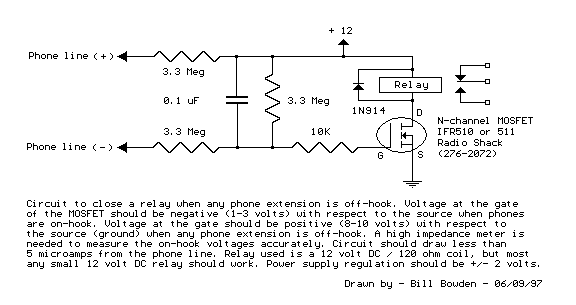
Circuit to close a relay when any phone extension is off-hook. Voltage at the gate of the MOSFET should be negative (1-3 volts) with respect to the source when phones are on-hook. Voltage at the gate should be positive...
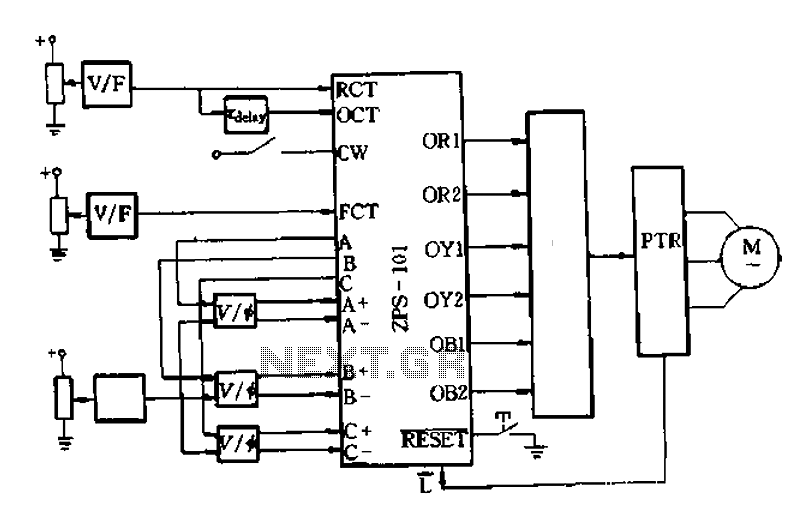
An AC-DC-AC circuit utilizes a power transistor as a switching device with analog control, as recommended in the wiring diagram of Figure 6-10. This circuit generates a voltage-controlled oscillator (VCO) using OCT and FCT, with RCT available for OCT...
The hardware design for USB is quite minimal, which is advantageous. However, it quickly becomes apparent that the simplicity of the hardware design leads to complex communication and control software, which will be explored further in the theory and...