
Battery-Saving Disconnect Switch

The circuit is designed to protect the battery from over-discharge by disconnecting it from the load when the voltage drops to a critical level. The use of a high-side floating-source MOSFET (Q1) allows for efficient switching with minimal voltage drop across the device when it is in the ON state. The current consumption of the circuit is low, drawing only 500 µA during operation and reducing to 8 µA when idle, which helps to extend battery life.
The voltage thresholds, VU and VL, are determined by the resistors R1, R2, and R3, which form a voltage divider that monitors the battery voltage. The circuit requires that the input voltage (V+) exceeds a certain threshold (VO) for the voltage detector IC1 to activate IC2. This ensures that the circuit only operates when there is sufficient battery voltage available.
IC2, a dual charge-pump inverter, is responsible for generating a higher voltage for driving the gate of Q1. The charge-pump configuration, which includes capacitors (C1 and C2) and diodes, effectively multiplies the input voltage to create a gate drive voltage that can exceed the battery voltage, allowing Q1 to turn on fully.
The hysteresis implemented in the circuit, with a threshold difference of approximately 0.5 V between VL and VU, prevents rapid toggling of the switch during minor fluctuations in battery voltage. This feature ensures stability in the operation of the circuit, allowing it to disconnect at 3.1 V and only reconnect when the voltage recovers to 3.6 V.
The design also accounts for the ON-resistance of Q1, which increases as the battery voltage decreases. This is critical for maintaining efficient operation; even at the threshold voltage, the drop across the switch remains low (30 mV at 300 mA load), ensuring minimal energy loss. Resistor R4 plays a vital role in ensuring that Q1 turns off completely by providing a discharge path for C2, thus facilitating the proper operation of the circuit and enhancing its reliability. At a predetermined level of declining terminal voltage, the circuit disconnects the battery from the load and halts potentially destructive battery discharge. Ql, a high-side, floating-source MOSFET, acts as the switch. The overall circuit draws about 500 when the switch is closed and about 8 when it"s open. The values of ii, R2, and R3 set the upper and lower voltage thresholds, Vv and VL, according to the relationships For the circuit to start, V+ must exceed VO. The voltage detector IC1 then powers IC2, but only while V+ remains above VL. Otherwise, IC2 loses its power, removes gate drive from Ql, and turns it off. IC2 is a dual chaige-pump inverter that normally converts 5 V to + 10 V. Capacitors CI, C2, and the two associated diodes form a voltage tripler that generates a gate drive for Ql that is approximately equal to two times the battery voltage.
With the values in the schematic, the circuit disconnects 3-cell Nicad battery from its load when V+ reaches a VL of 3.1 V. Approximately 0.5 V of hysteresis prevents the switch from turning on immediately when the circuit removes the load; V+ must first return to Vu, which is 3.6 V.
The gate drive declines as the battery voltage declines, cause the ON-resistance of Ql to reach a maximum of approximately 0.1, just before V+ reaches its 3.1-V threshold. A 300-mA load current at that time will cause a 30-mV drop across the disconnect switch. The drop will be 2 to 3 mV less for higher battery voltages. Resistor R4 ensures that Ql can adequately turn off by providing a discharge path for C2.
Related Circuits
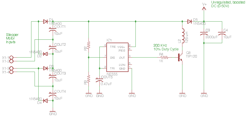
The circuit depicted in the schematic below represents an enhanced generator electronics system. It is an unregulated switcher designed to maximize sound output while ensuring prolonged CPU operation. This circuit efficiently transfers electrical energy from the generator, outperforming traditional...
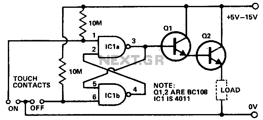
Touching the on contacts with a finger brings pin 3 high, turning on the Darlington pair and supplying power to the load (transistor radio, etc.). Q1 must be a high-gain transistor, and Q2 is chosen for the current required...
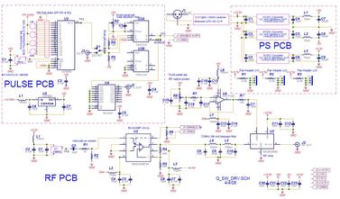
The Q-Switch driver for an old YAG laser failed. A replacement was over $1000, so a custom driver was built for less than $300 (see picture and schematic below). The specifications required were at least 20W into a 50-ohm...
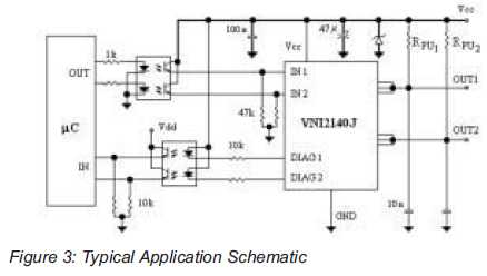
An integrated solution for two output channels that simplifies design and enhances reliability. The device, the VNI2140J, integrates on-chip two 45V Power MOSFET channels with a typical Rds(on) of 80mOhm at 25 degrees Celsius. The VNI2140J is a highly integrated...
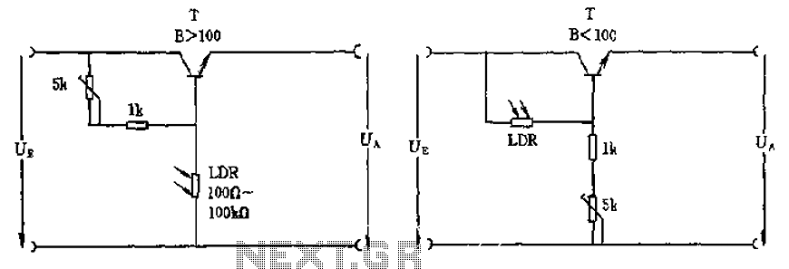
The circuit depicted involves a photoresistor (LDR) connected to a transistor, which operates at either a high or low level based on light conditions. The amplification factor of the transistor is 100, which is adequate for the application. The...
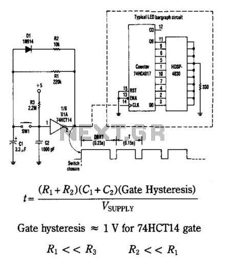
This circuit generates an output pulse when the pushbutton SW1 is pressed. It also functions as a hysteresis gate oscillator. Diode D1 and resistor R2 introduce asymmetry into the circuit. The delay before repeat time (DBRT) is influenced by...