
Bedside lamp with CD production delay

The described circuit utilizes a bistable trigger mechanism, which allows for two stable output states. The activation of switch SB transitions the output from one state to another, effectively functioning as a toggle switch. The timing characteristics of the circuit are adjustable by modifying the resistance or capacitance values of R3 and C2, which directly influence the delay time of the monostable circuit.
The inverters V and f, connected in parallel, ensure that the circuit can drive higher loads, improving the overall performance and reliability of the output signal. The zero-trigger SCR circuit, composed of transistors VT and associated resistors, is designed to control the operation of lamp H. The SCR remains in a conductive state when triggered and will turn off when the triggering signal is removed, allowing for efficient control of the lamp based on the circuit's input conditions.
Powering the circuit with 220V AC involves a voltage reduction through resistor R8, which limits the current flowing into the rectification stage. The diodes VD4, VD5, and VD6 serve to convert the AC voltage into a stable 6V DC, ensuring that the entire circuit operates within safe voltage levels while providing sufficient power for all components. This design emphasizes reliability and efficiency, making it suitable for various applications where bistable switching and delayed timing are required.FIG inverter I, II and R1, R2, CI and SB constitute bistable trigger switch, each time the switch SB, the anti- phase II level to the output of a change. Composition R3, C2, VD 1 inverting clamor I, t monostable delay circuit, adjust the value of the entire R3 or C2 can change the delay time of the circuit. Inverters V, f used in parallel to increase their ability to drive. VT transistors and peripheral resistors vs SCR zero trigger circuit, when vs turned on the lamp lit H: vs turned off, the lamp H goes out.
220V AC power via a resistor R8 buck, diode VD4, VD5 rectifier, VD6 stable regulated output voltage DC 6V for the use of the entire circuit.
Related Circuits

The 555 integrated circuit (IC) is utilized in a delay circuit configuration. It transitions from a high to a low output state when a button (SB) is pressed. The output remains high for a specified delay period before transitioning...
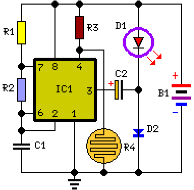
This circuit functions as a night lamp when a wall mains socket is unavailable for plugging in a continuously operating small neon lamp device. To minimize battery consumption, it utilizes a single 1.5V cell, and a simple voltage doubler...

This is a portable, high-power incandescent electric lamp flasher. It functions as a dual flasher (alternating blinker) capable of managing two independent 230V AC loads (bulbs L1 and L2). The circuit is entirely transistorized and operates on battery power....
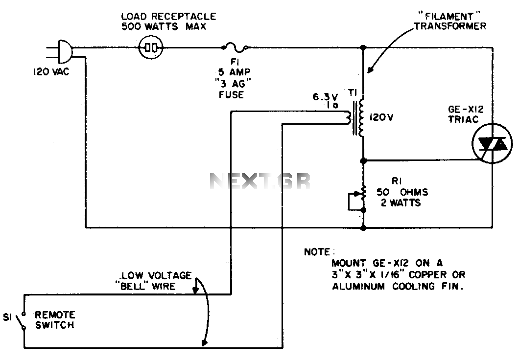
The circuit utilizes the primary current of a small 6-volt filament transformer to control a triac and activate the load. When switch S1 in the 6-volt secondary of the transformer is open, a small "magnetizing" current flows through the...
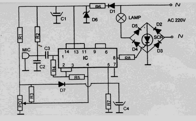
This 220 Volt disco lamp circuit is not a voice switch (VOX), as it cannot differentiate between musical sounds and human voices. Instead, it functions as a sound-activated device. An interesting application of this circuit is to control the...
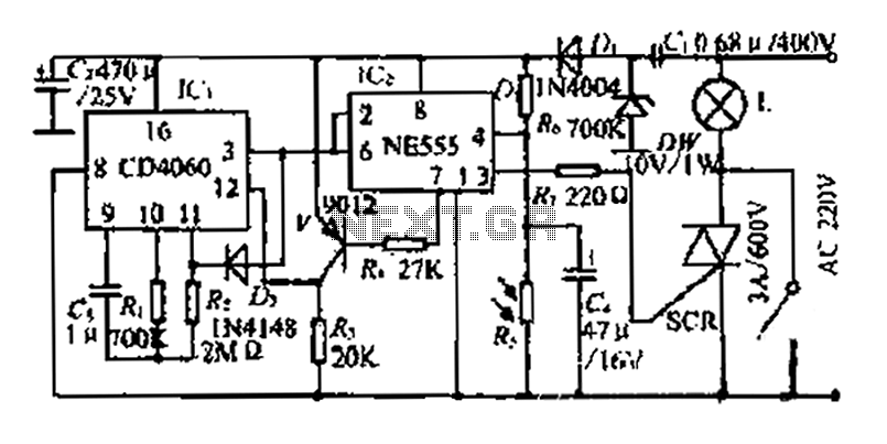
A photosensitive daytime electricity circuit utilizes a very small positive voltage. It features a 555 timer IC with four pins, including a reset pin that operates at low voltage. The circuit includes a bidirectional thyristor (iSCR) that controls lighting,...