
Bipolar dc-dc converter requires no inductor

The circuit utilizes two inverters, Ula and Ulb, to establish a stable 20-kilohertz square wave oscillator. The output from these inverters is essential for driving the power field-effect transistors (FETs), Q2 and Q3. The arrangement of these FETs in a push-pull configuration allows for efficient switching, where Q2 and Q3 take turns conducting, thereby optimizing power delivery to the load.
Diodes D2, D3, and resistors R4, R5, R6, and R7 are employed to shape the square wave output from the inverters. This shaping is crucial for ensuring that the waveform is suitable for driving the FETs effectively. The use of diodes in the circuit helps to rectify and clip the output waveform, providing the necessary voltage levels for the FETs to operate efficiently.
When Q2 conducts, it allows current to flow through Cout, which in turn activates diode D4. This process generates a positive voltage at terminal A, with the level of this voltage being stabilized by zener diode D5. Zener diodes are specifically chosen for their ability to maintain a constant voltage across their terminals, thus providing a reliable reference voltage for the circuit.
On the other hand, when Q3 is activated, it induces a negative charge on Cout, leading to the conduction of diode D7. This action results in a negative voltage being developed at terminal B, with its magnitude determined by zener diode D6. The configuration of D6 ensures that the negative voltage remains stable and within desired operational parameters.
Overall, this circuit design effectively demonstrates the use of oscillators, FETs, and zener diodes in generating and controlling voltage levels, showcasing a practical application in power electronics and signal processing.Inverters Ula and Ulb form a 20-kilohertz oscillator whose square wave output-further shaped by D2, R4, and R5 and by D3, R6, and R7—drives power field-effect transistors Q2 and Q3. The p-channel and n-channel FETs conduct alternately, in al push-pull configuration. When Q2 conducts, the positive charge on Cout forces diode D4 to conduct as well, which produces a positive voltage, determined by zener diode D5, at terminal A.
Similarly, when Q3, in its turn conducts, the negative charge on Cout forces D7 to do so as well. A negative voltage, therefore, develops at terminal B, whose level is set by D6.
Related Circuits
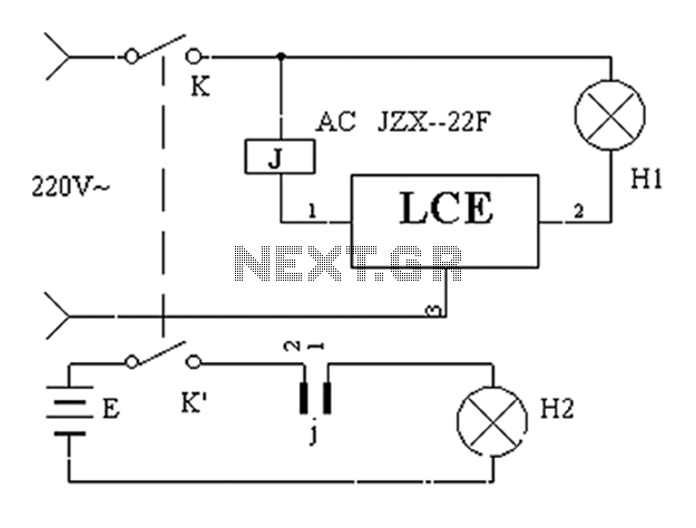
The application circuit operates the device as illustrated below, allowing for intermittent lighting in specific situations (e.g., during surgery). It utilizes an LCE module for blackout emergency lighting, which activates automatically after a power failure, ensuring uninterrupted illumination. In...
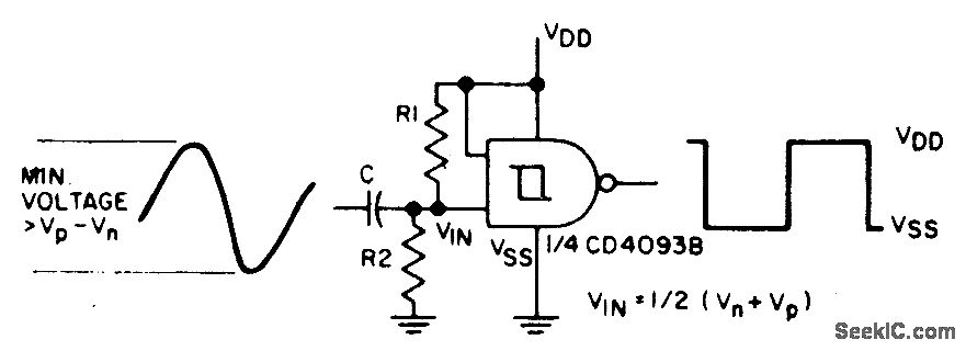
The sine input is AC coupled by capacitor C. Resistors R1 and R2 bias the input midway between Vn and Vp, the input threshold voltages, to provide a square wave at the output. The circuit described utilizes an AC coupling...
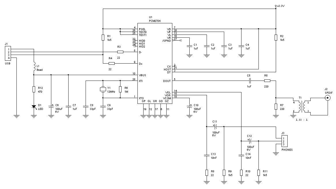
Is there a source for a schematic for a USB to SPDIF converter, similar to those offered by Empirical Audio? The concept is appealing, but the price of $500 is quite high. A USB to SPDIF converter is a device...
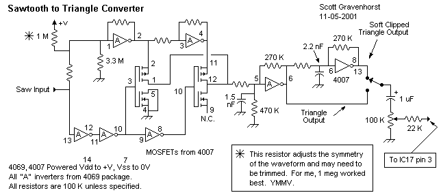
This wave shaper needs an input saw that goes from Vss to (ideally) Vdd. It works well with the 4069 VCO designed by Ren? Schmitz. Any saw will work as long as the wave is centered halfway between the...
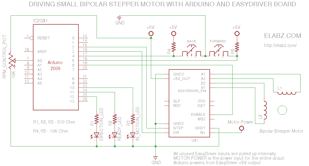
A simple circuit designed for testing bipolar stepper motors or for manual positioning using stepper motors. Schematics, Arduino sketch, and video are available. This circuit serves as a versatile tool for both testing and controlling bipolar stepper motors, which are...

The ICL7134B circuit is a bipolar input analog-to-digital (A/D) converter that employs two AM25L03 chips to create a 14-bit successive approximation register. The comparator features a two-stage amplifier, HA2605, which is utilized to mitigate settling time issues at the...