
14 Bit A-D Converter with ICL7134B

The circuit operates in a free-running mode when the HOLD/RUN input is low; however, it halts after completing a conversion if the pin is high at that moment. A low pulse can be used to restart the operation. The exit status provides information on whether the device is active, with the falling edge indicating the availability of new data. A unipolar version can be constructed by connecting the most significant bit (D13) of the ICL7134U to pin 14 of the first AM25L03, removing the reference inversion amplifier A4, and connecting to VRFM and VRFL.
The circuit design involves several key components and configurations that ensure accurate data conversion and reliable performance. The ICL7134B serves as the core A/D converter, utilizing its internal architecture to achieve high resolution and precision. The AM25L03 chips function as successive approximation registers, allowing for efficient conversion of analog signals to digital representations.
The HA2605 amplifier plays a critical role in enhancing the performance of the comparator by reducing settling time, which is essential for maintaining the integrity of the conversion process. The incorporation of an auto-zero circuit using the ICL7650 is particularly advantageous in applications subjected to varying temperature conditions, as it helps maintain accuracy by compensating for offset errors.
The clock circuit's design, utilizing TTL Schmitt triggers, is optimized for the differing settling time requirements of the initial and subsequent bits. This careful timing strategy ensures that the most critical bits are processed with the utmost precision, thereby improving overall conversion accuracy.
The HOLD/RUN input functionality provides flexibility in the circuit's operation, allowing it to either continuously convert data or pause and restart based on external control signals. This feature is particularly useful in applications where data acquisition needs to be synchronized with other system components.
The option to configure the circuit for unipolar operation expands its applicability, making it suitable for a wider range of signal types. By modifying the connections and removing specific components, the circuit can be adapted to meet the specific requirements of various measurement and control tasks.
Overall, the ICL7134B-based circuit represents a sophisticated solution for high-resolution analog-to-digital conversion, combining advanced components and thoughtful design to achieve reliable performance across diverse applications.The circuit ICL7134B base is a bipolar input AID converter broadband, using two AM25L03s to form a successive approximation register 14-bit. The comparator is a circuit with two stage amplifier HA2605 front, used to reduce the settling time problems in the pro summing node (see A020).
Warning nu11ing offset of this amplifier is needed and if wide temperature range operation is desired, an auto-zero circuit using a lCL7650 is probably desirable (see A053). The clock, using two gates TTL Schmitt trigger operates at a slower pace for the first 8 bits, where the settlement time is more critical than for the last 6 bits.
The line is short-cycle showed little tied at 15, if fewer bits are needed, it can be moved accordingly. The circuit will free run if the HOLD / RUN input low, but stops after performing a conversion if the pin is high at this time.
a low pulse will restart it. The exit status indicates whether the device is operating, and the falling edge indicates the availability of new data. Unipolar version can be built by typing the MSB (D13) on a ICL7134U to pin 14 on the first AM25L03, deleting the reference inversion amplifier A4, and attaching to VRFM VRFL.
The line is short-cycle showed little tied at 15, if fewer bits are needed, it can be moved accordingly. The circuit will free run if the HOLD / RUN input low, but stops after performing a conversion if the pin is high at this time.
a low pulse will restart it. The exit status indicates whether the device is operating, and the falling edge indicates the availability of new data.
Related Circuits
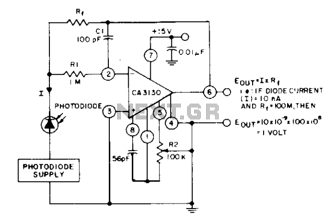
The circuit utilizes three CA3130 BiMOS operational amplifiers in an application that is sensitive to sub-picoampere input currents. It provides a ground-referenced output voltage that is proportional to the input current flowing through the photodiode. The circuit design employs three...
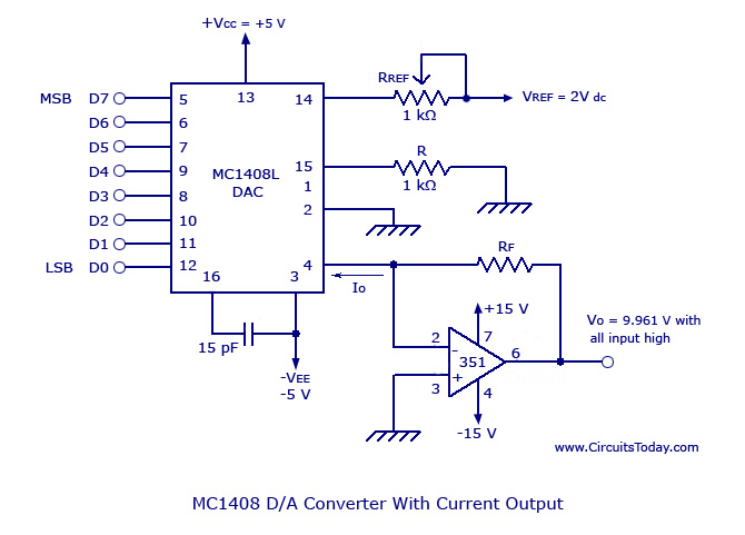
Monolithic/Hybrid Digital to Analog Converters using MC 1408 IC, SE/NE 5018, Specifications and Applications. Monolithic and hybrid digital-to-analog converters (DACs) are integral components in various electronic systems, facilitating the conversion of digital signals into corresponding analog voltages or currents. The...
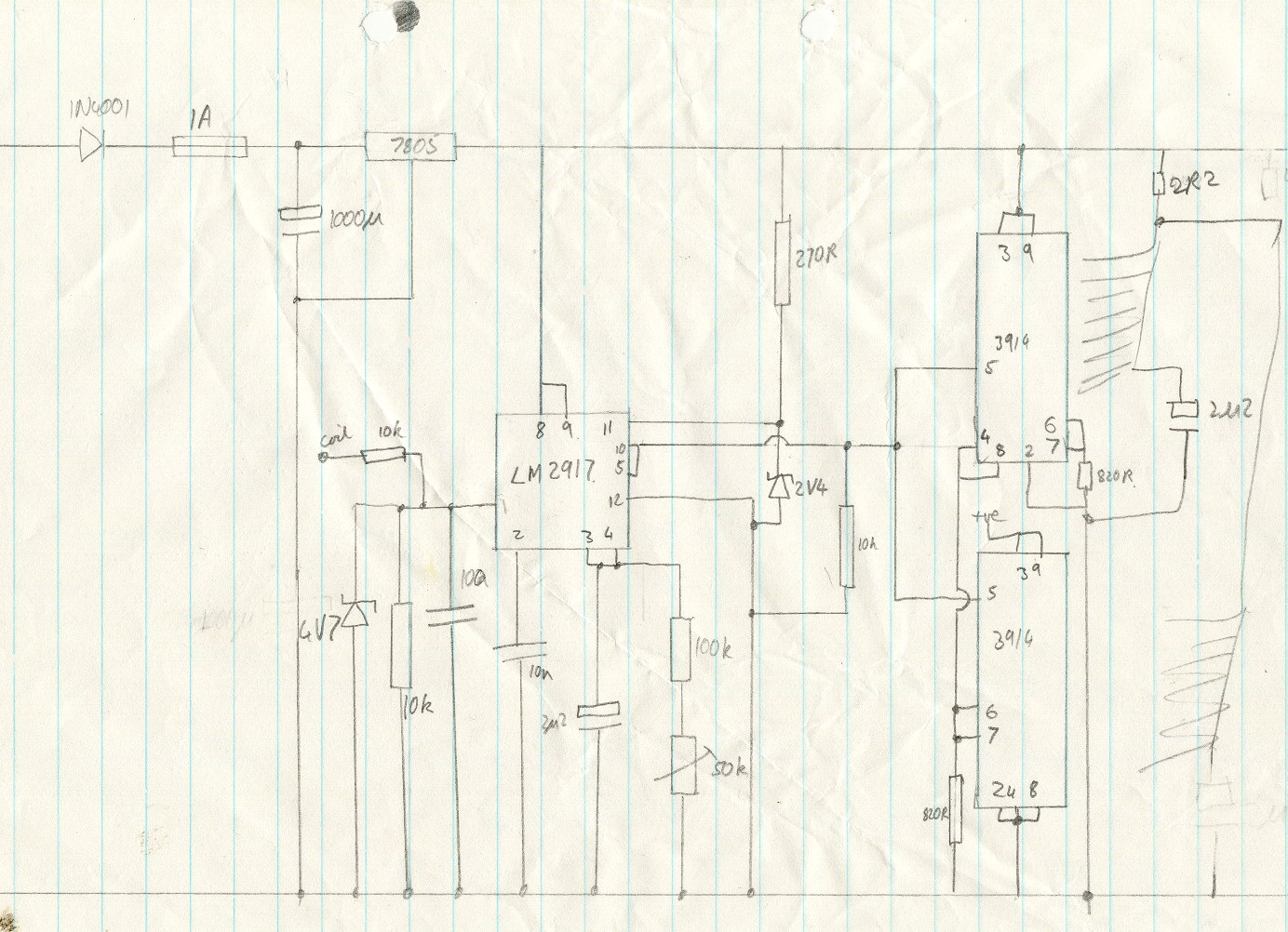
This circuit utilizes an LM2917 frequency-to-voltage converter. The input is connected to the low voltage side of the ignition coil, with various components designed to produce a full-scale output at 6000 RPM, corresponding to 12000 ignition pulses per minute,...
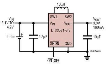
The LTC3531, LTC3531-3.3, and LTC3531-3 are synchronous buck-boost DC/DC converters that function with input voltages that can be above, below, or equal to the output voltage. The topology utilized in these integrated circuits (ICs) enables continuous power transfer across...
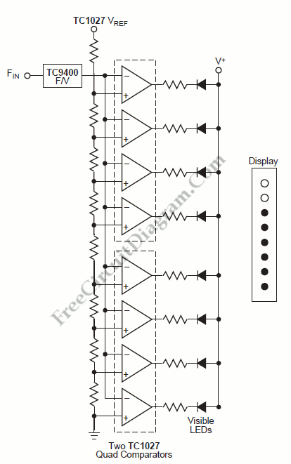
A tachometer can be constructed using the TC9400 in frequency-to-voltage (F/V) mode to convert frequency information (RPM) into a linearly proportional voltage. This voltage can then be compared to one of several comparators (in this example, using eight). The...
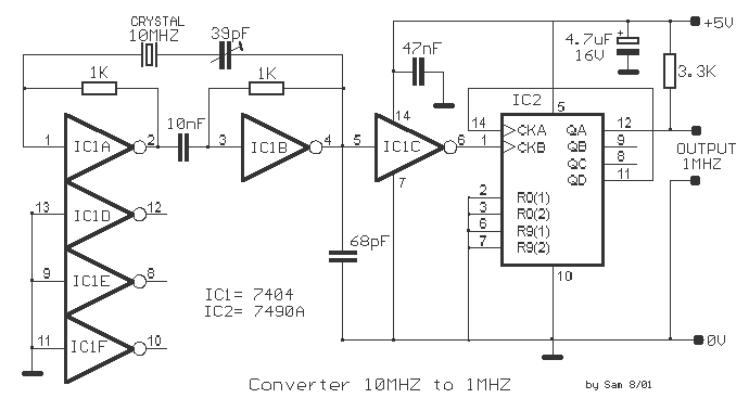
This circuit is an oscillator at frequency 10MHZ, using IC 1A and IC1B and a frequency divider. Using the IC2 it divides the pulses to 10. IC1C is a buffer. The variable capacitor 39pF is microtuning the frequency. The...