
Boost ConverterCircuit Based On The 555 IC

The Boost Converter is a type of DC-DC converter that steps up the input voltage to a higher output voltage while maintaining the same power level, subject to efficiency constraints. The circuit utilizes the 555 timer IC, which is a versatile and widely used integrated circuit in various applications, including timing, pulse generation, and oscillator functions.
In this specific configuration, the 555 timer is set up in astable mode, generating a square wave output. This pulse signal is used to control a switching device, typically a transistor, which connects and disconnects the input voltage to an inductor. As the transistor switches on and off, energy is stored in the inductor during the 'on' phase and released to the output during the 'off' phase, effectively increasing the voltage.
The essential components of the circuit include:
1. **555 Timer IC**: Configured to produce a pulse-width modulated (PWM) signal that controls the transistor.
2. **Inductor**: This component stores energy when the transistor is on and releases it to the output when the transistor is off.
3. **Diode**: A flyback diode is used to prevent back EMF from the inductor from damaging the transistor.
4. **Capacitor**: This component smooths out the output voltage, reducing ripple and ensuring a stable voltage supply.
5. **Resistors**: These are used to set the timing characteristics of the 555 timer and to limit the current through the circuit.
The circuit's design allows for flexibility in output voltage by adjusting the duty cycle of the PWM signal generated by the 555 timer. By varying the resistor and capacitor values in the timing circuit, the frequency and duration of the pulse can be modified, thus changing the output voltage level.
Overall, this Boost Converter Circuit based on the 555 IC is an efficient and cost-effective solution for applications requiring a higher voltage from a lower voltage source, utilizing readily available components.The following circuit shows about Boost Converter Circuit Diagram. This Circuit Based On The 555 IC. Featrures: only requires an `of the shelf` .. 🔗 External reference
Related Circuits

The first positive pulse from a classic 555-based oscillator is always 1.6 times longer than the subsequent pulses. This discrepancy arises because, during the initial cycle, capacitor C2 begins charging from 0 V. While this is typically not an...
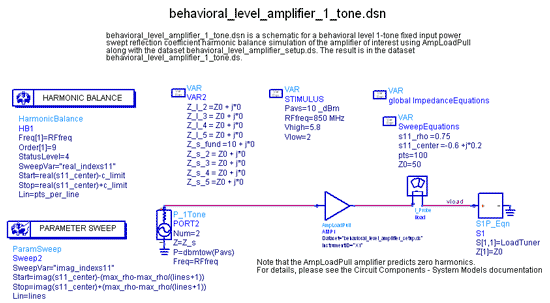
The AmpLoadPull project demonstrates the utilization of the AmpLoadPull and LoadPullSetup components in Advanced Design System (ADS). These components are part of the ADS behavioral model suite located within the System - Data Models palette. The schematic "circuit_level_amplifier_1_tone.dsn" represents...
Micro or analog? These days, it is becoming increasingly challenging to make a choice. The 555 timer has long been regarded as a benchmark for flexibility. How does it perform today? The 555 timer IC, originally introduced in 1972, remains...

Security has become a significant concern in today's world, leading to the availability of various security gadgets. This document introduces a simple touch alarm designed specifically for doors with metallic handles. The alarm functions exclusively on metallic handles and...

A pair of multi-range timers capable of timing periods up to 24 hours and beyond. Both versions are fundamentally similar, with the primary distinction being that Version 1 energizes the relay when the time expires, while Version 2 de-energizes...

The original FLED-based SE uses a flashing LED to drive a type 1 solar engine (you'll note that it's just like the Zener-based SE, but with a FLED in the starring role). The good news is that all the...