
Broadband frequency doubler

This circuit employs a switching differential amplifier configuration to achieve signal doubling. The amplifier operates in a linear region when the input signal at the carrier input is maintained below 25 mV peak, ensuring minimal distortion in the output. The selection of capacitor C is crucial; it should be chosen based on the operating frequency of the circuit to minimize reactance, thereby optimizing performance.
In scenarios where higher input signals are present, the use of a resistive divider is recommended. This technique allows for the attenuation of the input signal to a level suitable for the carrier input while enabling the full input signal to be utilized at the signal input. The resistive divider should be carefully designed to ensure that the voltage drop across the divider does not exceed the specified threshold for linear operation.
The output waveform integrity is paramount, and while levels approaching 50 mV peak can be accommodated, the resultant distortion must be assessed based on the application's requirements. It is essential to balance the input signal levels and the desired output fidelity to achieve optimal circuit performance.This circuit will double low-level signals with low distortion. The value of C should be chosen for low reactance at the operating frequency. Signal level at the carrier input must be less than 25 mV peak to maintain operation in the linear region of the switching differential amplifier. Levels to 50 mV peak may be used with some distortion of the output waveform If a larger input signal is available, a resistive divider may be used at the carrier input with full signal applied to the signal input.
Related Circuits
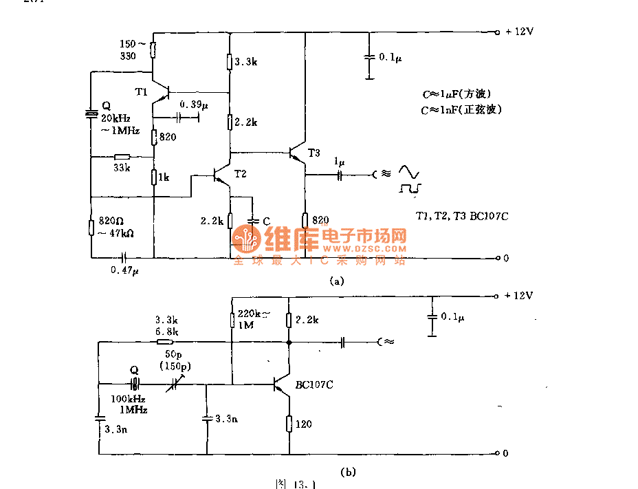
Figures (a) and (b) illustrate two basic oscillator circuits operating at 2 MHz. The circuit design allows for adjustment of the optimal operating point through testing. The two oscillator circuits depicted in the figures utilize different configurations to achieve stable...
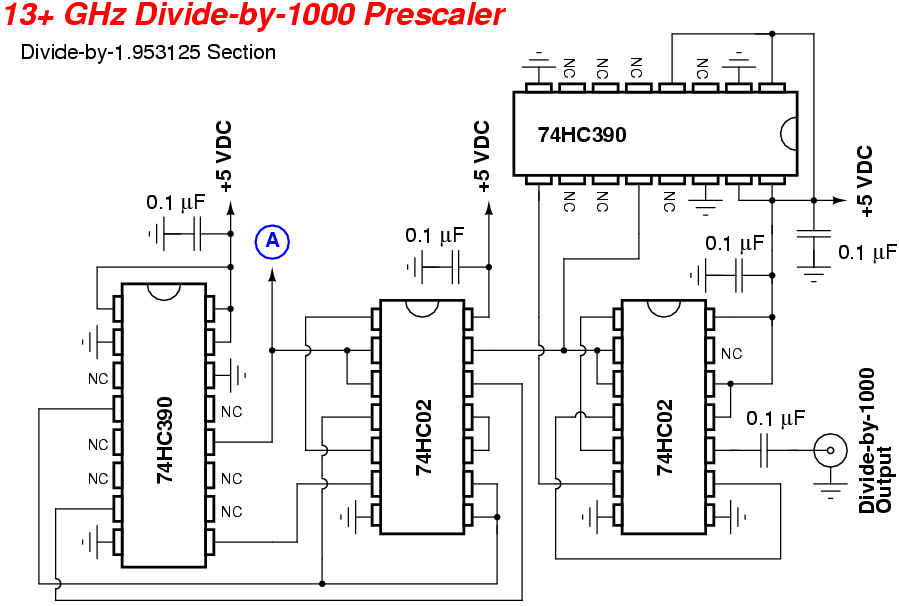
A straightforward "divide-by-1000" circuit was originally designed by Zeljko Bozic, S52ZB, in a 2006 issue of VHF Communications Magazine. This project aims to extend the range of older and more affordable frequency counters. Frequency counters capable of measuring up...
A wide range frequency meter is a useful tool for an electronics lab. This project describes a frequency meter based on the AT90S231 microcontroller that can measure input frequencies up to 50 MHz. The measured frequency is displayed on...

A function generator that operates within a frequency range of 0.1 Hz to 20 MHz can be easily constructed using the MAX038 integrated circuit chip. This describes a straightforward implementation of the device. The MAX038 is a precision waveform generator...
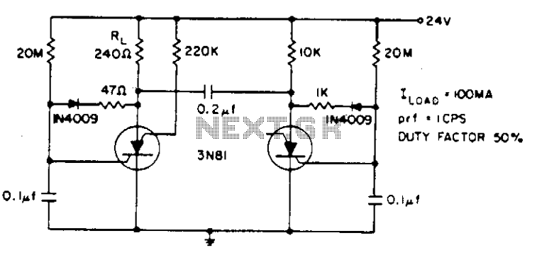
Electrolytic capacitors are not required to generate a 1 cps frequency. When the silicon-controlled switch (SCS) is triggered, the 0.2 µF commutating capacitor deactivates the other capacitor and charges its gate capacitor to a negative potential. The gate capacitor...
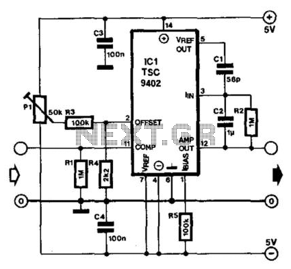
Teledyne Semiconductor's Type TSC9402 is a versatile integrated circuit (IC) capable of converting voltage to frequency and frequency to voltage. It is well-suited for use as an add-on unit for measuring frequencies with a multimeter, requiring only a few...