
buck converter design demystified

Buck converters are a type of DC-DC converter that efficiently reduce a higher input voltage to a lower output voltage while maintaining a high level of efficiency. They are widely used in various applications, including power supplies for microcontrollers, battery chargers, and LED drivers. The fundamental operation of a buck converter involves the use of a switch (typically a transistor), a diode, an inductor, and a capacitor.
The switching element alternates between the on and off states, controlling the energy transferred to the inductor. When the switch is closed, current flows through the inductor, storing energy in its magnetic field. When the switch opens, the inductor releases the stored energy to the output load through the diode. The capacitor smooths the output voltage, reducing ripple and providing a stable voltage to the load.
Key parameters to consider in buck converter design include the input voltage range, output voltage, output current, switching frequency, and efficiency. The inductor value can be calculated based on the desired output current ripple and the switching frequency. Similarly, the output capacitor value is determined by the acceptable voltage ripple at the output and the load transient response.
To optimize performance, it is essential to select components that can handle the required current and voltage ratings, and to implement proper layout techniques to minimize parasitic inductance and resistance. Additionally, feedback control mechanisms are often employed to maintain output voltage regulation under varying load conditions.
Overall, understanding the operational principles and design considerations of buck converters is crucial for engineers looking to implement these devices in efficient power management solutions.Though stepdown converters - buck converters - are extremely popular, the rules of thumb and calculations that speed their design can be hard to find.. 🔗 External reference
Related Circuits
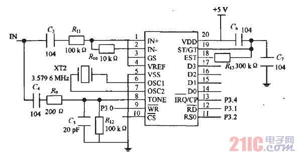
Precautions must be taken against low safety coefficients, as the applicable space for security measures continues to shrink. With advancements in science and technology, innovations such as magnetic door sensors, touch-type systems, radar monitoring, and infrared detection have emerged,...
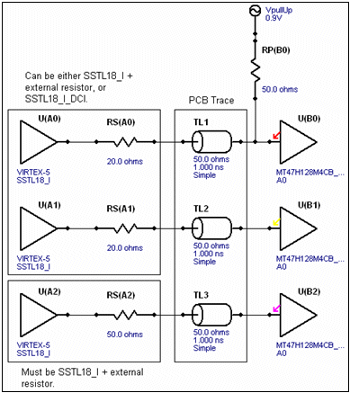
This article discusses practical techniques for incorporating "correctness by design" in DDR2 interfaces from a Signal Integrity (SI) perspective, utilizing the current generation of available design tools. It analyzes common DDR2 design errors and the trade-offs between various popular...

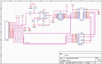
The photodiode current-to-voltage converter circuit employs three CA3130 BiMOS operational amplifiers, designed for applications that require sensitivity to sub-picoampere input currents. This circuit generates a ground-referenced output voltage that is directly proportional to the input current flowing through the...
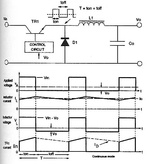
The buck converter circuit serves as the foundation for various similar circuits, known as forward converters. The configuration of the buck converter, along with its input and output voltages, is illustrated in Figure 1. This circuit is typically connected...
Mixed Analog/Digital Design Using Split Power and Ground Planes. The following example illustrates the design of a circuit that incorporates both analog and digital components. It features multiple power planes and a single ground plane that is divided into...
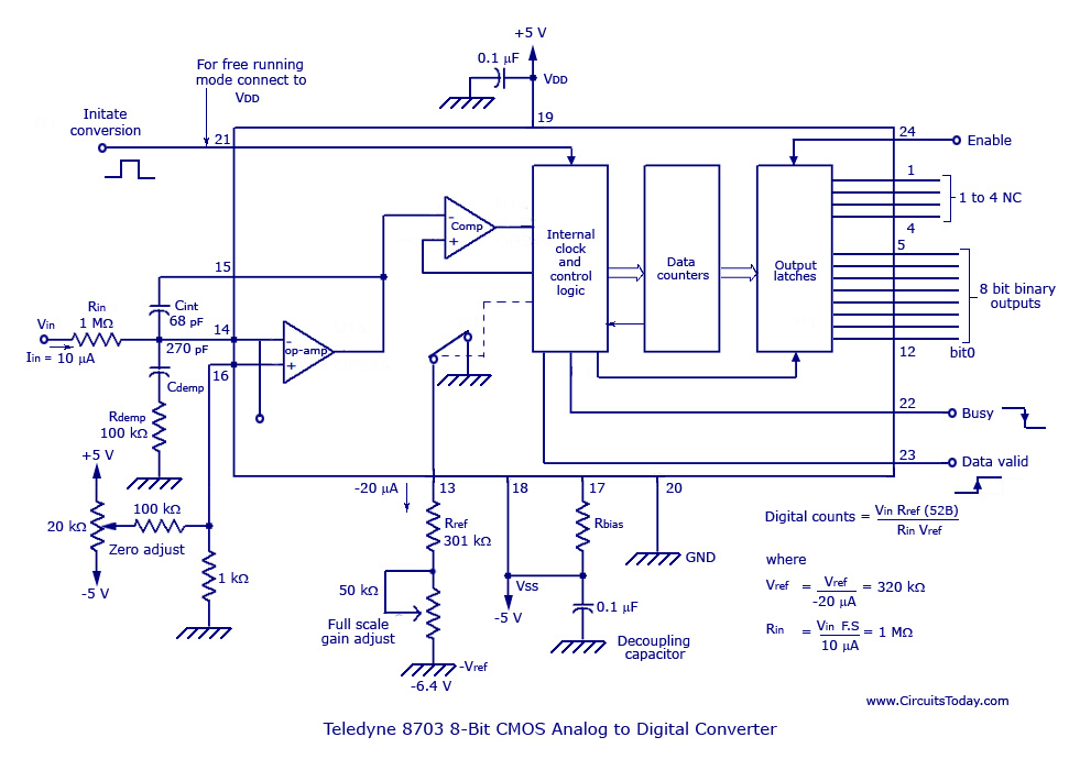
The basic analog to digital (A/D) converter circuit has been previously explained. In addition to this, various types of monolithic analog to digital converters exist, including the integrating A/D, integrating A/D with three-stage outputs, and the tracking A/D with...