
How to design 65nm FPGA DDR2 memory

The article emphasizes the importance of "correctness by design" in DDR2 interfaces, particularly from a Signal Integrity perspective. This approach focuses on preemptively addressing potential design errors, which can significantly impact the performance of DDR2 memory systems. By analyzing common pitfalls encountered in DDR2 designs, engineers can make informed decisions regarding design alternatives that balance performance and reliability.
The schematic representations in the figures provide critical insights into effective design practices. The preferred usage model depicted in Figure 1 highlights the optimal configuration for DDR2 interfaces, ensuring that the memory chip operates as the driver and the FPGA as the receiver. This configuration allows for the effective use of the FPGA's DCI capabilities, which are essential for maintaining signal integrity across the bi-directional data lines.
Figures 1 and 2 not only illustrate the preferred topology but also showcase variations that are often employed in real-world design scenarios. Understanding these variations can help engineers avoid common mistakes and improve the robustness of their designs. The inclusion of input switching thresholds as dashed blue lines serves as a reference point, aiding in the evaluation of the receiver's performance under different conditions.
The use of Mentor Graphics' HyperLynx software to generate eye diagrams is a valuable tool for visualizing the signal integrity of the DDR2 interfaces. Eye diagrams provide a graphical representation of the signal quality and timing characteristics, allowing designers to assess the impact of their design choices on overall system performance. By utilizing eye diagrams generated with specific parameter settings, engineers can fine-tune their designs to achieve optimal signal integrity and reliability in DDR2 memory applications.This article presents practical techniques for incorporating "correctness by design" in DDR2 interfaces, from a Signal Integrity (SI) perspective, using the current generation of available design tools. Some common DDR2 design errors are analyzed, as well as the tradeoffs between some popular design alternatives.
Several possible address/control t opologies for DDR2 shown in Fig 1, while several possible data topologies are illustrated in Fig 2. In order to make use of the FPGA`s on-die digitally controlled impedance (DCI), the memory chip was made the driver and the 65nm FPGA device the receiver on the bi-directional data lines. The top schematic diagram in Fig 1 shows the preferred and recommended use model, while the other figures illustrate variations often attempted in regular design practice.
The input switching thresholds of the receiver are shown as horizontal dashed blue lines for reference. The color of the "probe" arrows in Fig 1 and Fig 2 correspond to the colors of the associated traces in Fig 3 and Fig 4, respectively.
Mentor Graphics` HyperLynx software was used to generate eye diagrams with the following parameter settings: 🔗 External reference
Related Circuits

VD represents the voltage drop across the diode, while VTrans indicates the voltage drop across the transistor. The boundary between continuous and discontinuous operation occurs when the output current (io) is zero. A primary consideration in converter design is...
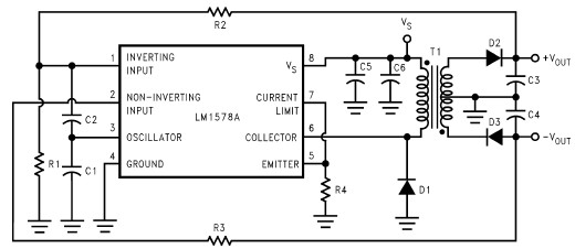
This RS232 power supply circuit diagram is a simple RS-232 line driver power supply that operates from an input voltage as low as 4.2V and delivers an output of ±12V at ±40 mA with an efficiency of better than...

This application note aims to introduce filter designers to the basics of active filter design using monolithic integrated circuit operational amplifiers (op-amps). It includes a table of transfer functions and network equations for high-pass, low-pass, band-pass, and band-reject filters....
Observing and addressing the phase adjustment issues in electric transmission lines manually poses significant challenges, particularly in recording and normalizing three major problems. This design encompasses both software and hardware components, developed over an extended period. It is intended...
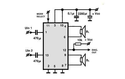
A simple Class B power amplifier can be constructed using the TDA8560 audio integrated circuit (IC). The TDA8560 amplifier features an internally fixed voltage gain, ensuring excellent channel balance. This audio amplifier project is capable of delivering dual 40-watt...
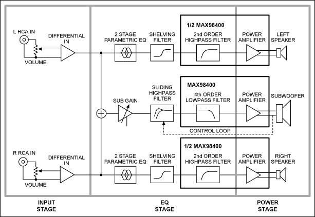
This reference design demonstrates the MAX98400 Class D audio amplifier in a stereo audio docking station application. The demo box is a powered speaker dock that drives a speaker system consisting of 2-inch satellite speakers and a 5-inch subwoofer. The...